
The "PSPeakV Regulator" for High Voltage B+ Regulation
Primary Side Peak Voltage Regulator
Regulated 500Vdc 220mA from a pair of 230V Transformers
Regulated 300Vdc 105mA from a $42 Digikey Transformer.
June 2026, Ver 0.7
This is another Idea I wanted to share before a "Bleeping Truck" gets me
CTRL-F5 to load latest version
SCR regulators tend to be noisy because of the fast voltage and fast currents that flow when SCR triggers. The currents in the SCR will be very high and voltage changes on the output capacitor will also spike when the SCR fires and charges the output capacitors. The noise made by an SCR regulator can be difficult to control.
This
regulator works by turning a primary side switch off when the output
voltage hits a given peak output voltage. This doesn't give perfect
regulation, but it is good enough for most applications. This
regulation method is fast. It responds in just 1/2 of a line cycle.
The switching action does generate some noise, but it is mostly
capacitive coupled noise. With an SCR, the noise is both magnetic and
capacitively coupled.
To control noise in this circuit, we slow the turn off voltage rise
times by placing capacitors across the switching nodes on the primary
side. The secondary side snubber on the transformer also becomes
important for it will have the fastest moving voltage waveforms if it
is not correctly snubbed. The primary side capacitors work the best
with one across the line input and one across the transformer.
The primary side switch uses a "zero voltage" turn on circuit that to
decide when to turn the IGBTs on. This reduces power losses and
reduces the noise generated. If the zero voltage is measured across
the two primary side switches to primary ground, the circuit becomes
extremely sensitive to the values of the snubbers and bypass
capacitors. If the zero voltage is measured across the pair IGBTs that
make the primary side switch, the switching is no longer as sensitive
to the capacitor values. Splitting the snubber capacitor into
two parts makes a quieter voltage controller, but it causes a little
more power loss. It was less than 1/4W of extra loss if memory serves
me correctly.
The Primary side switch can have current sense resistors in it to help
control fault currents and to providing a "soft-start" on the output
by slowly ramping the current limit up from zero to its final value.
The lower the resistance of the transformer's primary (the lower the
regulation), the higher we have to set the peak current limit.
By switching on the primary side of the transformer instead of the
secondary side, the switches only need to handle the peak currents and
peak voltages that occur on the primary side. A 1200V 200W regulated
supply and a 300V 200W supply typically have all the same parts on the
primary side of the controller. The difference between 1200V and 300V
will be in the output capacitors, output diodes and the transformer
used..
The downside to this regulation method is that you need a separate power transformer for B+ than what you use for the filaments. While it takes more room to do this, I'm finding that two smaller standard transformers costs less than the equivalent all-in-one transformer. If you want to use an all-in-on transformer, the Half Baked Clap-R regulator could be a choice for you if you desire HV regulation.
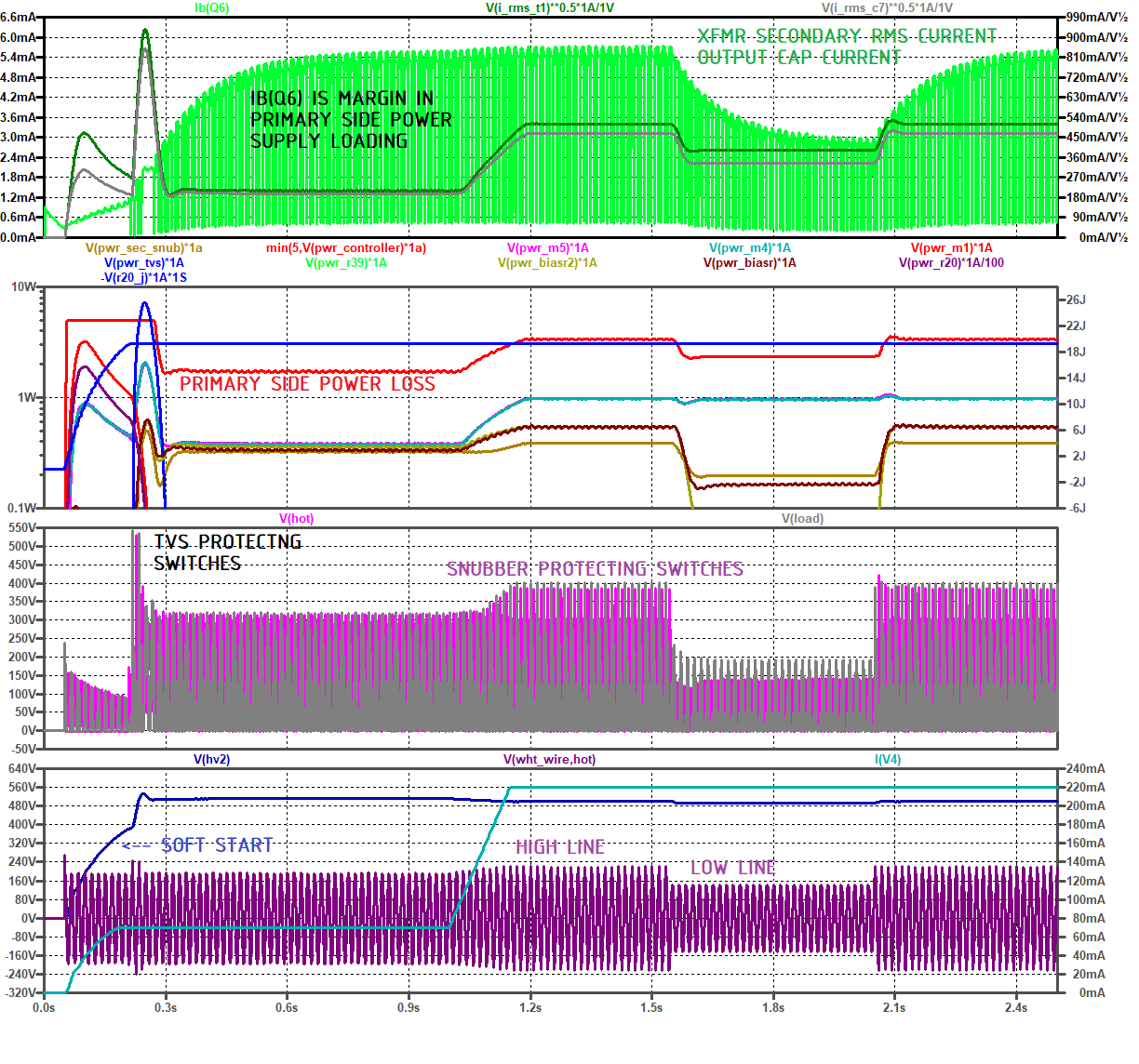
1. The power loss in our tubes stays the same no matter what the line voltage does.
2. We can add an "electronic" high voltage turn-on delay to let the cathodes warm-up before the high voltage is applied.
3. We can add a "soft-start" that slowly raises the high voltage output to lower tube stresses as the amp finds its bias point.
4. We can protect against really high output voltages that occur if the power supply is powered on with no load (no tubes, intermittent tubes or cold tubes) This alone saves size and cost in the parts we need in our designs.
5. With a moderate effort, we can make the output short circuit proof.
6. With a current limiting short circuit protection circuit, we can put the Biggest Farad Capacitor (BFC) that we can fit in our chassis and have a chance not causing rolling blackouts when we turn our amplifier on.
If you use a BFC, make sure you have something like the Discharginator, a BFC auto-discharge circuit. If you go the BFC route, increase the size of the heatsink on the IGBT output switches so that the junction temperature stays less than about a 40C rise under worst case conditions. How big of a heatsink? Hey, I'm giving away the LTSPICE files on this, use them to find out!
I kept the simple 120V EMI filter in the baseline schematic because it makes writing this page easier. The filter consists of 30uH in the L21 occurring from a decent length run of ROMEX in the wall and a 20uH physical inductor.
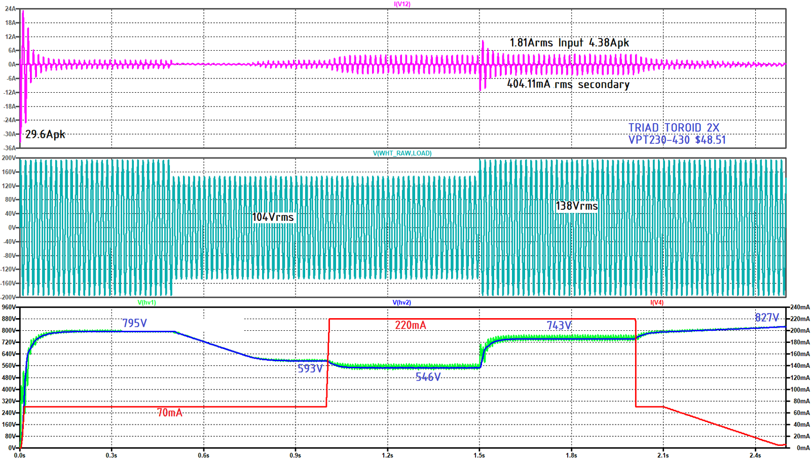
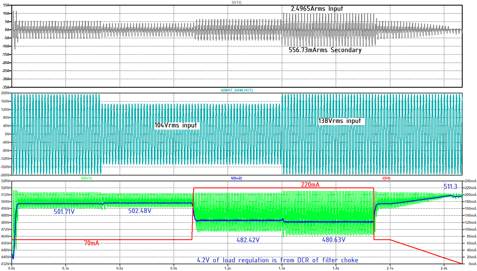
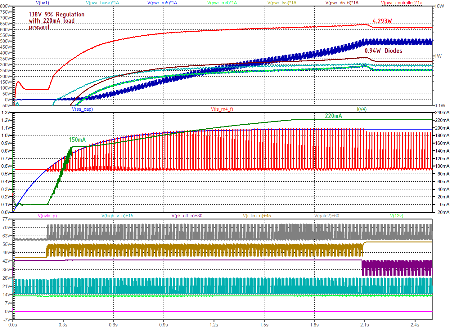
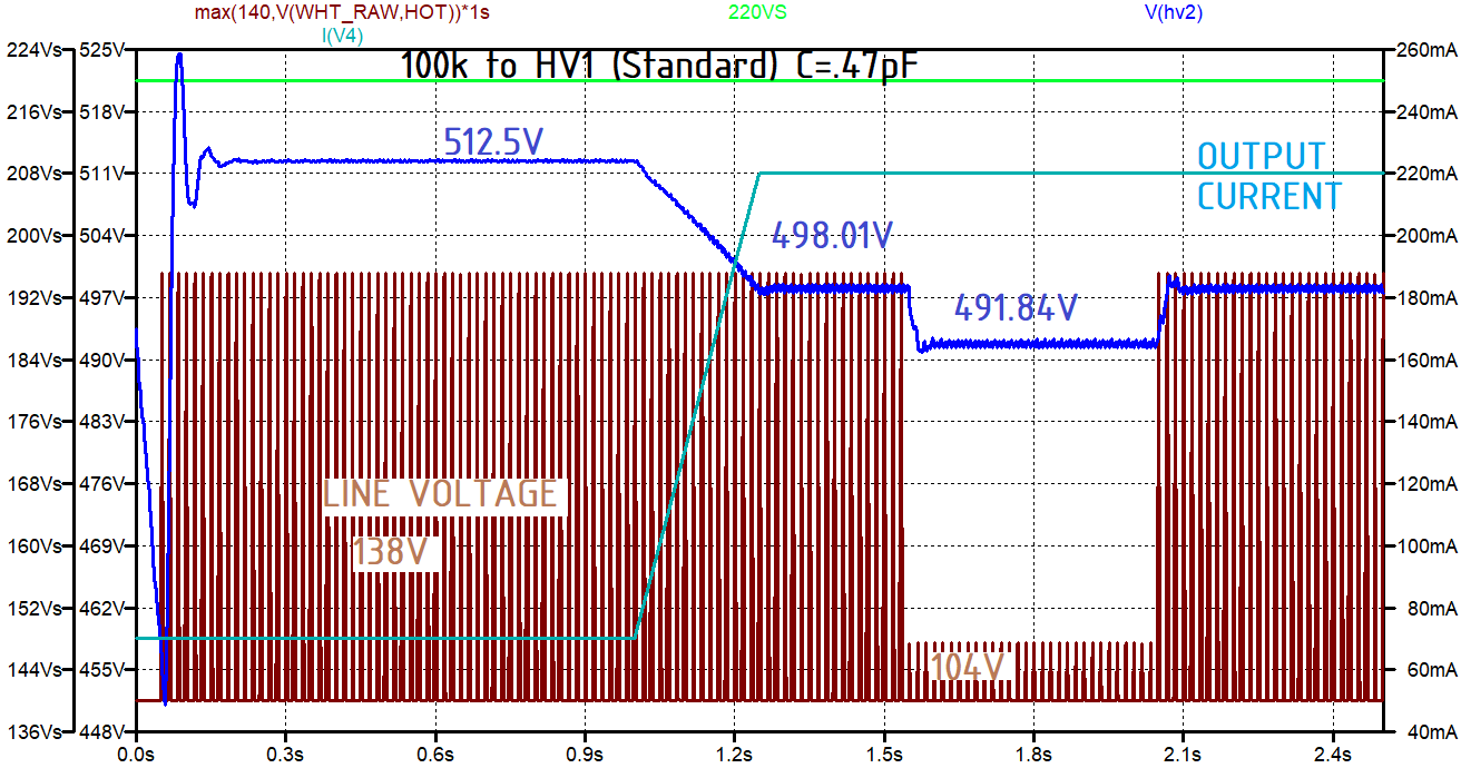
From 70mA load to 220mA load we get a 48V drop in the output voltage.
From 138Vac input to 104Vac input we get a 202V change in the output voltage.
At no load, the 546V min output peaks up to 827V. This peaking is a part "Killer" in some designs.
s
irms_sec: RMS(i(v9))=0.392473 FROM
1.80617 TO 1.85617
hv2_min: MIN(v(hv2))=589.397 FROM 0.1 TO 2.5 (was 545.7V)
hv2_max: MAX(v(hv2))=928.44 FROM 0.1 TO 2.5 (was 837V)
hv2_nom_ll: AVG(v(hv2))=669.618 FROM 0.9 TO 0.95
hv2_max_ll: AVG(v(hv2))=590.174 FROM 1.4 TO 1.45
hv2_max_hl: AVG(v(hv2))=813.179 FROM 1.9 TO 1.95
pout: AVG(i(v4)*v(hv2))=178.905 FROM 1.80617 TO 1.85617
pin: AVG(-i(v12)*v(wht_raw,load))=210.484 FROM 1.80617 TO 1.85617
loss: pin-pout=31.5792 (was 17.6W with 9% regulation transformer)
Irms_sec: RMS(i(v9))=0.406403 FROM
1.80617 TO 1.85617
hv2_min: MIN(v(hv2))=545.658 FROM 0.1 TO 2.5
hv2_max: MAX(v(hv2))=826.913 FROM 0.1 TO 2.5
hv2_nom_ll: AVG(v(hv2))=593.895 FROM 0.9 TO 0.95
hv2_max_ll: AVG(v(hv2))=546.72 FROM 1.4 TO 1.45
hv2_max_hl: AVG(v(hv2))=743.831 FROM 1.9 TO 1.95
pout: AVG(i(v4)*v(hv2))=163.643 FROM 1.80617 TO 1.85617
pin: AVG(-i(v12)*v(wht_raw,load))=181.291 FROM 1.80617 TO 1.85617
loss: pin-pout=17.6477
Irms_sec: RMS(I(V9))=0.540325973446
FROM 1.80106698301 TO 1.85106698104
hv2_min: MIN(V(HV2))=482.208221436 FROM 0.1 TO 2.5
hv2_max: MAX(V(HV2))=513.685058594 FROM 0.1 TO 2.5
hv2_nom_ll: AVG(V(HV2))=504.909203153 FROM 0.9 TO 0.95
hv2_max_ll: AVG(V(HV2))=484.910769922 FROM 1.4 TO 1.45
hv2_max_hl: AVG(V(HV2))=483.131518049 FROM 1.9 TO 1.95
pout: AVG(I(V4)*V(HV2))=106.292004023 FROM 1.80106698301 TO
1.85106698104
pin: AVG(-I(V12)*V(WHT_RAW,LOAD))=157.435942912 FROM 1.80106698301 TO
1.85106698104
loss: PIN-POUT=51.1439388883 (33.5W to regulate)
This is not the final version of the digital delay regulator, but it is representative of the results. The regulator regulates the peak output voltage, not the average.
When the line voltage drops, the output voltage actually goes up a tiny bit. This is because the output voltage is moving slower at the crest of the input sinewave. Having a longer duration near the peak of the line voltage causes the peak output voltage to the average output voltage to be closer together and thus the average output voltage rises.
When the load current drops, the regulated peak voltage stays the same but the ripple voltage on the first capacitor increases. This drops the average output voltage and is the major driver for the load regulation we get with this circuit. The DC output voltage from the first capacitor is "Vpeak" - "Vpkpk"/2. If we switch at 510Vpk and have 12Vpp of ripple in the first capacitor, the DC voltage is about 504Vdc.
If the first capacitor after the diode bridge is made lower ESR or high capacitance, the output regulation improves. Too big of a capacitor in the output results in not being able to read the peak output voltage correctly and the output ends up being noisy. The end message is "DON'T GET GREEDY", it won't end well for the circuit performance. Remember, "Better is the enemy of Good". (But what is good enough???)
The output worked down to about 10mA load (511V out). It also worked down to no load without getting too ugly (<511V out).
For a lower output power, the design can be "re-tuned" to get better performance at light loads. Likely all that needs to change is to increase the value of the current sense resistor.
For a higher output power, it will also have to be re-tuned with larger capacitor values on the transformer, the current sense resistor will have to decrease and IGBT and Diode losses will have to be checked..
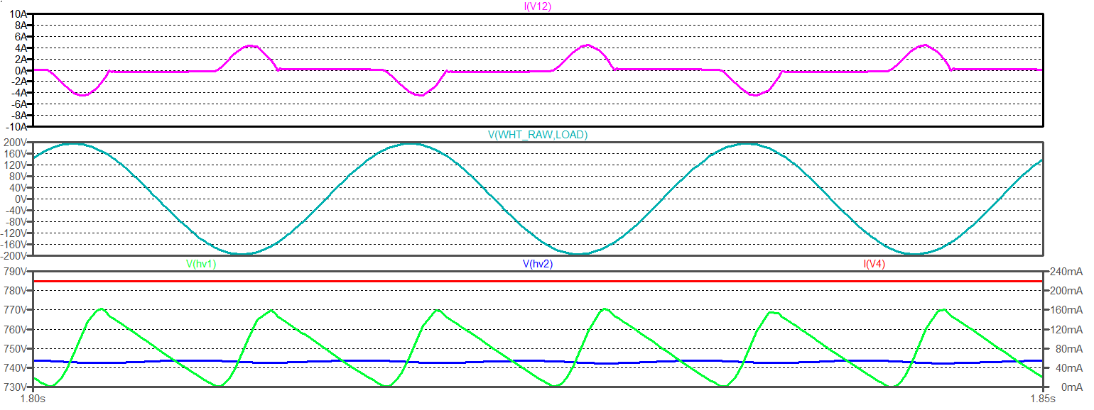
The Voltage Scale has Changed
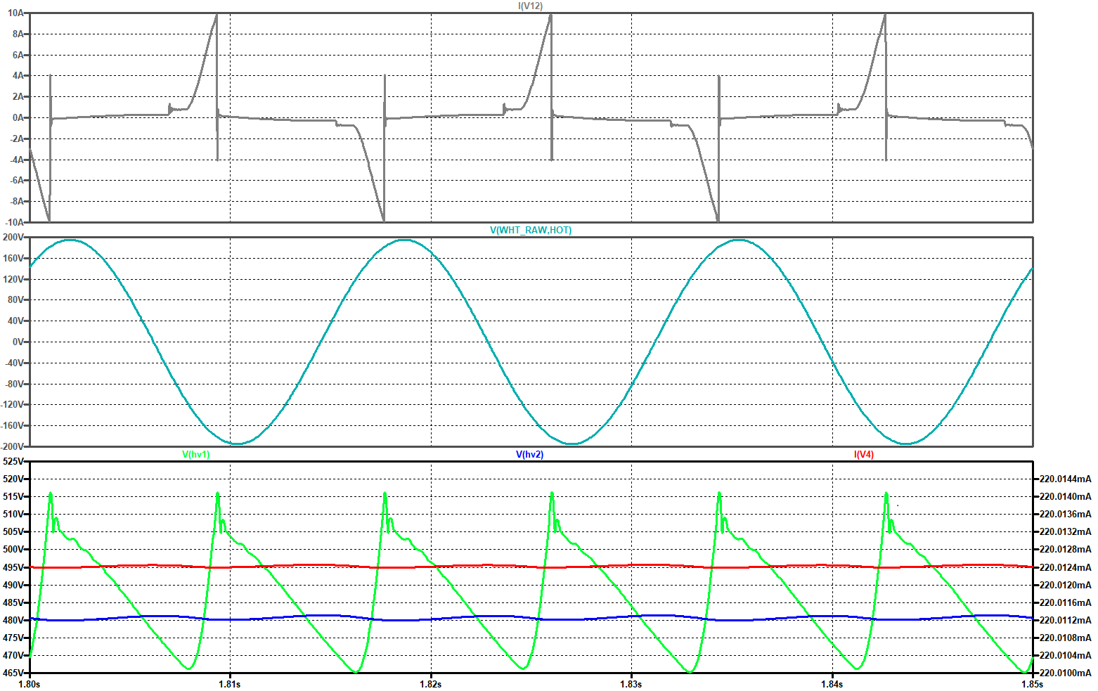
We can zoom-in on the high line and maximum load area see what is going on. We see that the input primary currents are higher than without the regulator, but we have regulation!
The narrow spikes on HV1 can be reduced with a Film Capacitor across the aluminum capacitor banks.
The spikes in current on V12 are from how we get regulation. The circuit has a side effect of narrowing up the current duration as part of the voltage peak detect operation. Since the same average current must be passed, the peak current must rise to maintain that average.
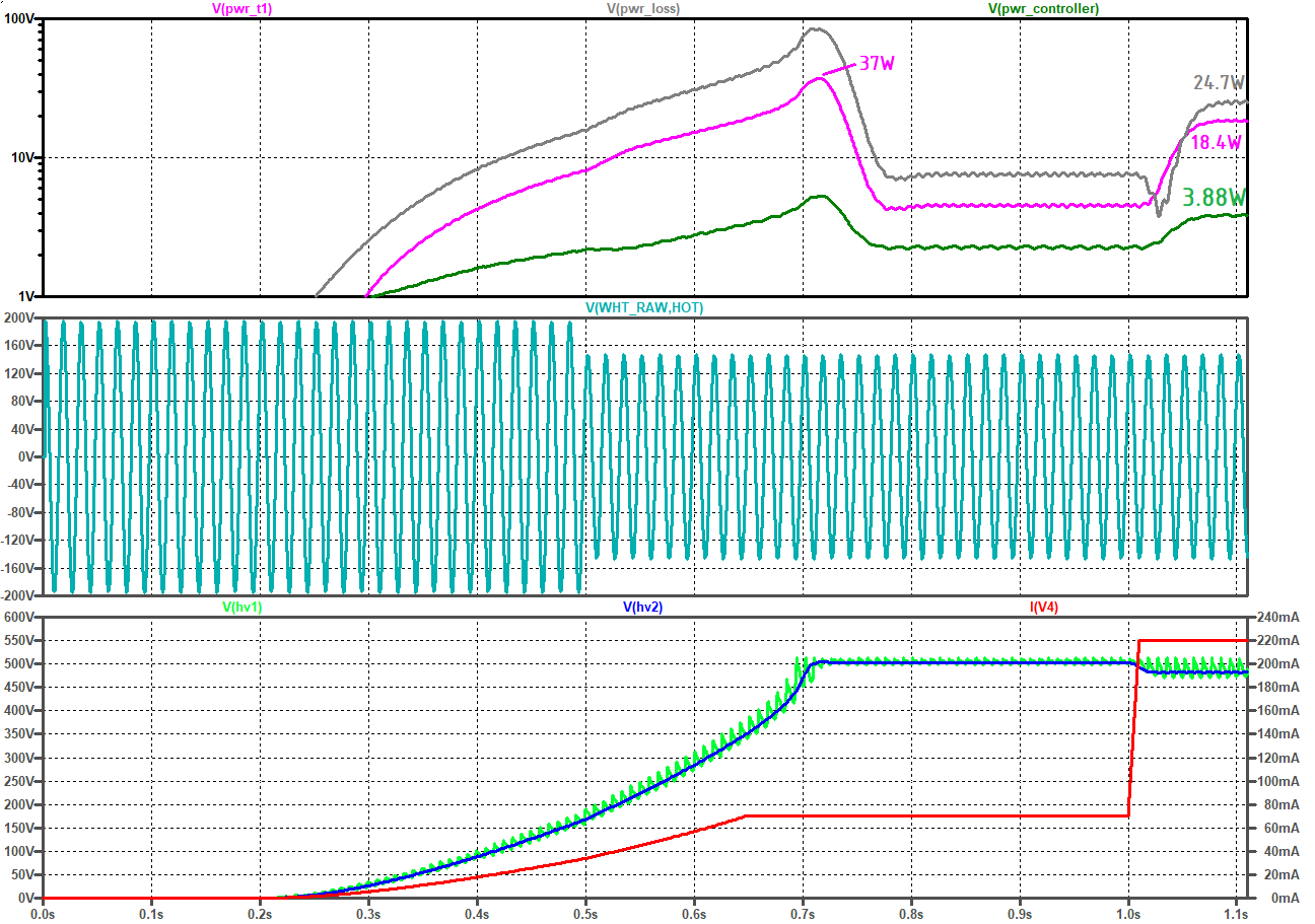
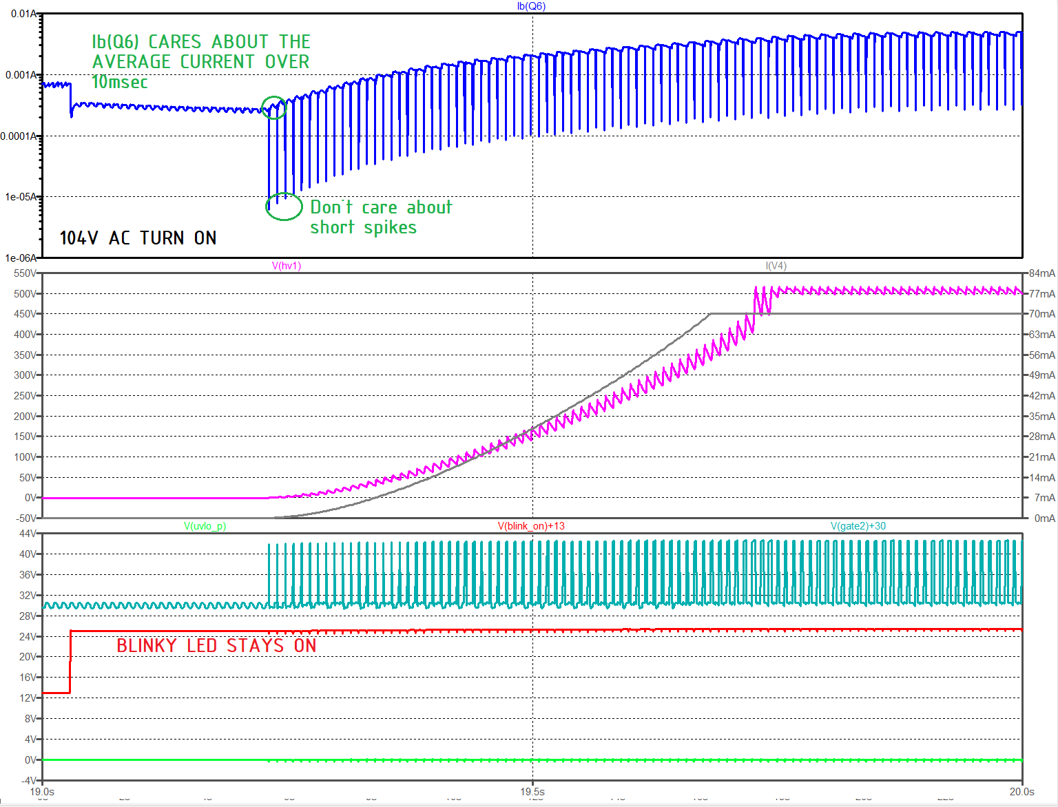
Before the final circuit tuning, the soft-start profile (without warm-up delay) looks as shown below with the soft-start capacitor = 15u. This is with a 70mA load present on the 500V during turn on.
We can make the rise time take twice as long by changing the 15uF capacitor value. At four times as long I'd start to worry about the power transformer. Most of the soft-start power is lost in the power transformer. The transformer's power loss doubles at the peak of the inrush and quickly settles down. Normal full load power loss in the transformer is expected to be 23.5W. The power transformer has a lot of thermal mass, a short term 2X overload isn't going to damage it. The plot below would fall under "short term."
With the same regulator, the model predicts that the 25% regulation transformer's output will perform the same as the 9% regulation transformer. The noise on the output will be slightly different and the 25% regulation part will have higher power losses. The 25% regulation transformer throws away 25% of the voltage internal to the part. It makes sense a part that only throws away 9% of the output voltage internally would be more efficient. Why sell a 25% regulation part? It takes more material (i.e. it costs more) to make a 9% regulation transformer over a 25% one. See Lowell Quist on transformer regulation A 25% regulation transformer will also have a lower inrush current when turning on when compared to 9% parts
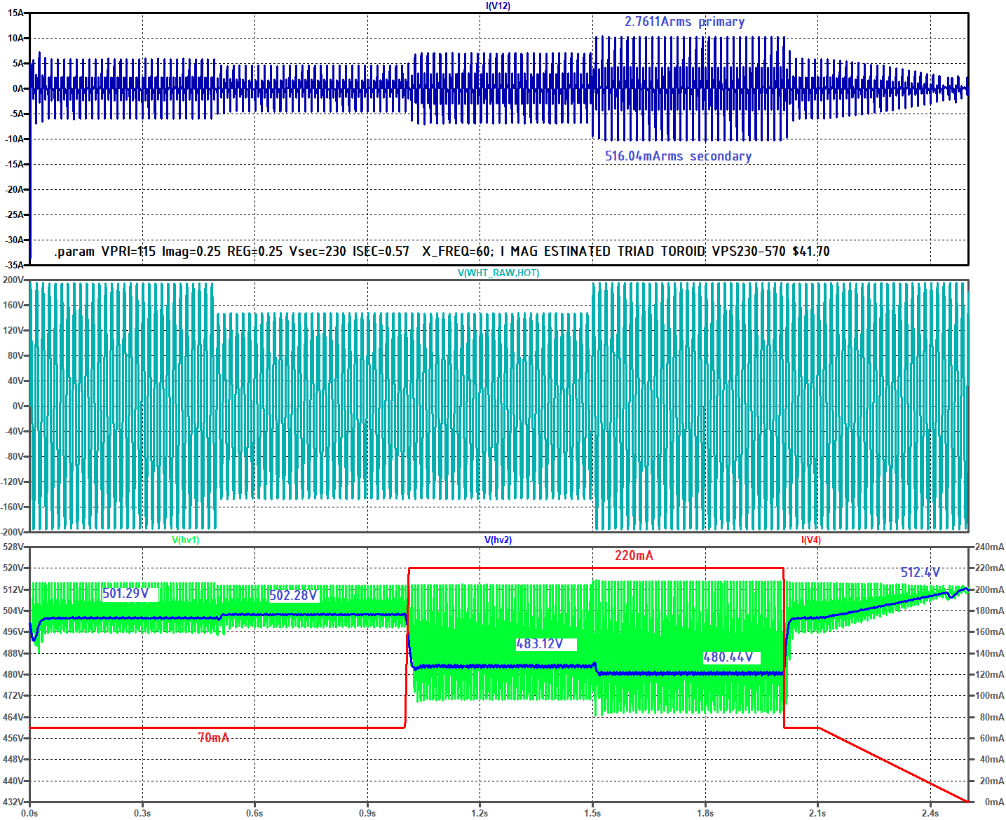
Irms_sec: RMS(i(v9))=0.516039 FROM
1.80093 TO 1.85093
hv2_min: MIN(v(hv2))=479.529 FROM 0.1 TO 2.5 (Was 479.7 on 9%)
hv2_max: MAX(v(hv2))=512.415 FROM 0.1 TO 2.5 (Was 511.3 on 9%)
hv2_nom_ll: AVG(v(hv2))=502.601 FROM 0.9 TO 0.95 (Was 502.5 on 9%)
hv2_max_ll: AVG(v(hv2))=483.107 FROM 1.4 TO 1.45 (Was 482.3 on 9%)
hv2_max_hl: AVG(v(hv2))=480.436 FROM 1.9 TO 1.95 (Was 480.6 on 9%)
pout: AVG(i(v4)*v(hv2))=105.702 FROM 1.80093 TO 1.85093
pin: AVG(-i(v12)*v(wht_raw,load))=174.89 FROM 1.80093 TO 1.85093
loss: pin-pout=69.1883 (Was 51.1W on 9%)
This data is not from the final version, but it is close enough. It is from using the 9% regulation transformer.
Cbias = 0.39uF set to 90%
R bias = 2x 1.2K series
D bias = 1N4148
D IGBT = GB8J bridge
IGBT = irg4pc50fd
The "Bird's Eye" view of the losses on Ver 8 B 138V input 220mA out is:
|
Power Loss |
32.545 |
Watts |
|
PWR in T1 |
24.233 |
Watts |
|
PWR in Dout +Cout_ESR +Sec_snubber |
3.446 |
Watts |
|
PWR Controller |
4.885 |
Watts |
|
Missing |
-0.019 |
Watts |
|
% missing |
-0.059 |
|
The controller is where we can get in trouble with hot parts. These numbers are steady state. At turn on, during soft-start, during short-circuit etc. the power loss in the IGBTs, Diodes across the IGBTs, the TVS, the transformers etc can increase.
The GBU diode bridge may need a small heatsink because of transients.
The IGBTs will need a small heatsink because we need to treat them gently thermally.
The Controller losses are those from after the input LC filter to where we hit the transformer. The losses are as follows:
|
Digital V8_B 138Vac |
Watts |
|
|
PWR_CTRL |
4.8851 |
< -- Total |
|
|
|
|
|
M4 |
0.5499 |
0.22 out |
|
M5 |
0.5561 |
0.22 out |
|
D5+D6 (GBJ8) |
0.7755 |
|
|
Rbias Diodes |
0.0206 |
|
|
R39 |
0.0023 |
|
|
BiasR |
1.0660 |
2.4K 0.39*0.9 |
|
BiasR2 |
1.1820 |
2.4K 0.39*0.9 |
|
PWR_TVS |
0.0057 |
|
|
Primary
Side |
0.3170 |
All IC’S |
|
Zero V resistors |
0.0704 |
|
|
LED PWR |
0.0000 |
Included |
|
Isense R |
0.3294 |
|
|
Correction
for |
0.0105 |
|
|
|
|
|
|
PWR Missing |
-0.0002 |
|
|
% missing |
0.0000 |
|
|
mA missing on +12 |
0.0000 |
|
Other interesting points to know about:
0.5433 Irms T1 secondary
0.5073 Irms C7 output capacitor
0.4246 W in the "R3" snubber on the input LC tank
0.3393 W in top secondary snubber C snub = 22nF
255 V pkpk Vbias use > 200Vac part
520.V pkpk C81/C80 22nF snubber use >400Vac part
23.35 Vdc C Turn_on_Delay
13.17 Vdc 12V
13.5741 mA I(R6) unit running
9.0016 mA Ib(Q6) unit running
After writing the table above, I found that I didn't save the final corrections in the LM2901B model. It was drawing 1mA too much from the power rail. After correcting this, I discovered that I could drop Cbias from 0.39uF (an X capacitor style) to 0.22uF and still have 350uA min into the base of Q6 at 104Vac low line. I'm willing to accept this margin. Instead of re-running all the plots and re-tabulating the data, I just added an "Oops" correction factor in the table above.
350uA is acceptable because as soon as the switching stage start chopping, the ringing from the chop adds current to the 12V rail and the Q6 drive margin goes up.
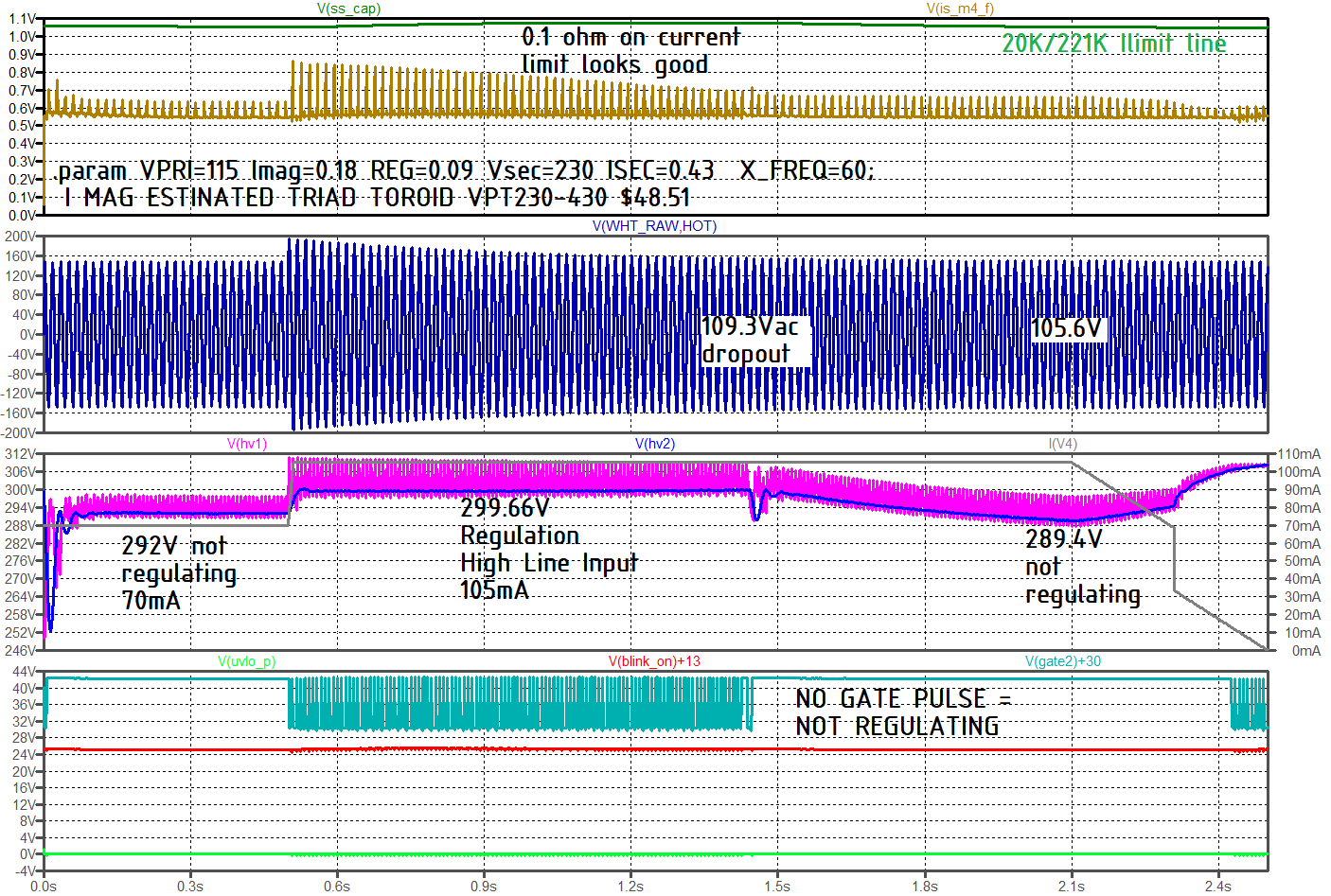
With a 221K to 20K ohm over-current set point and a 0.05 ohm current sense resistor, the digital regulator preformed adequately into a short of the load side of the output LC tank. The following measurements were with the GBJ8 diodes across the irg4pc50fd IGBTs
At 104V input
Ioutput = 517mA
Controller loss = 3.7039W (Cbias = 0.22u Rbias = 750 ohm)
GBJ8 Bridge: = 0.77888W
M4+M5: 0.53767W + 0.532332W = 1.07W total
9% regulation transformer loss = 38.654W (We're pushing the part a little.)
At 138V input
Ioutput = 482.31mA
Controller loss = 3.499W (Cbias = 0.22u Rbias = 750 ohm)
GBJ8 Bridge: = 0.6309
M4+M5: 0.45188W + 0.4514W = 0.90W total
9% regulation transformer loss = 34W
The Soft-Start actually is more stressful on the controller than a zero ohm short. The controller's losses peak right at the transition between soft-start and regulation.
At 104V input, 0.05 ohm I sense, 20K/221K current limit resistors, the soft-start stresses peak as shown below
Ioutput = 220mA or 1.8K ohm, which ever is less current.
Controller loss = 5.816W for ~130msec (Cbias = 0.22u Rbias = 750 ohm)
GBJ8 Bridge: = 1.953W for ~80msec
M4+M5: = 2.43W total for ~90msec
9% regulation transformer loss = 60.2W for ~120msec
"~" is the old shorthand for "approximately."
At 138V input, 0.05 ohm I sense, 20K/221K current limit resistors, the soft-start stresses peak as shown below
Ioutput = 220mA or 1.8K ohm, which ever is less.
Controller loss = 4.31W for ~180msec (Cbias = 0.22u Rbias = 750 ohm)
GBJ8 Bridge: = 0.934W for ~130msec
M4+M5: 0.53767W + 1.243W total for ~180msec
9% regulation transformer loss = 32.8W for ~390msec
The time of the overload was measured from halfway up from "steady state" on rising edge to the peak and from the peak to "steady state" on the falling edge.
Low line power stresses were worse than at high line for normal start-up and for a short. Weird isn't it.
For the soft-start, what the IGBTs and GBJ8 diodes need is a bit of thermal mass. A large 1" long screw through the GB8J likely will be enough thermal mass. A less than 15C/W heatsink shared by M4 and M5 would provide enough mass and cooling that they are not at risk.
The transformer is iron and copper, it will have plenty of thermal mass. Copper has a huge thermal mass per unit volume.
If we beef up the GBJ8 diodes to a GBU3510 size diode, we should be able to skip heatsink and the added thermal mass on the bridge rectifier diode.
The GBJ8 diode runs about 1.15V at 20 amp peak and has a 26C/W Rthja (56C rise in a short, 21C nominal), the GBU35 diode runs at about 0.95V and has a 22C/W Rthja (estimated 39C rise into a short and 15C rise normal.) We may want to build with the GBU35 and avoid adding a heatsink.
If you look at the high line "RED" trace above, the peak IGBT current, the actual current is running very close to the over current limit (blue). It is too close for comfort. In the final build, not in this web article, I'd change the current reference divider from 20K and 221K to be closer to 24.9K and 221K for 46% more peak current. That is "if" everything behaves with 46% more peak current. While I was at it, I'd change the other 20Ks to 24.9K.
The 25% regulation transformer doesn’t make it any better.
Increasing the current limit from being set by a 20K/221K divider to being set by 24.9K/221K at 104V input we get:
Ioutput = 890.28mA (The output LC tank will run at 2.2x current, 5X normal temperature rise.)
Controller loss = 14.59193W (Cbias = 0.22u Rbias = 750 ohm)
GBJ8 Bridge: = 1.70522W (OK, but hot)
M4+M5: 1.20014W + 1.17741W = 2.38W total (OK on a 9C/W heatsink)
TVS Power = 6.71864W ( That's a lot unless we put a lot of copper on the TVS' lands. Increasing the 3.3uF will help.)
9% regulation transformer loss = 101.21W I secondary =1.175rms (2.7 times rated, too much)
The results say that increasing the current limit by 46% without re-tuning all the other value a bad idea. When time permits, I’ll re-run it with the 20K set to 21.5K,
Whenever possible, I avoid part values where the decimal point has moved to be used if they are in the same package size. So no 22.1K and 221K both in 1206. If the 22.1k was 0805, I’d buy it. NEVER use a 221k 1% 100ppm/C and 221k. 0.1% 25ppm/C in the same package. You are just begging Murphy to get them swapped. With capacitors, this is difficult to enforce. But no 1% caps and 5% or 10% caps in same package with same value.
b_i_ibq6_min_____:
MIN(Ib(Q6))=0.000480048882309
FROM 4.4811656161 TO 4.49783228277
b_i_load_v4______: AVG(I(V4))=0.890093616224 FROM 4.4811656161 TO
4.49783228277
b_i_r6___________: AVG(I(R6))=0.00936398250412 FROM 4.4811656161 TO
4.49783228277
b_irms_c7________: AVG(V(I_RMS_C7)**0.5)=0.937276521283 FROM
4.4811656161 TO 4.49783228277
b_irms_input_____: AVG(V(I_RMS_INPUT)**0.5)=4.54626938491 FROM
4.4811656161 TO 4.49783228277
b_irms_t1________: AVG(V(I_RMS_T1)**0.5)=1.17510995938 FROM 4.4811656161
TO 4.49783228277
b_p1_t1__________: AVG(V(PWR_T1))=101.215459335 FROM 4.4811656161 TO
4.49783228277
b_p2_p_d_c_out___: AVG(V(PWR_D_C_OUT))=10.1521777312 FROM 4.4811656161
TO 4.49783228277
b_p3_ctrl________: AVG(V(PWR_CONTROLLER))=14.5919384445 FROM
4.4811656161 TO 4.49783228277
b_p4_m4__________: AVG(V(PWR_M4))=1.20014888598 FROM 4.4811656161 TO
4.49783228277
b_p4_m5__________: AVG(V(PWR_M5))=1.1774181108 FROM 4.4811656161 TO
4.49783228277
b_p6_d5_6________: AVG(V(PWR_D5_6))=1.70522488697 FROM 4.4811656161 TO
4.49783228277
b_p7_biasr2______: AVG(V(PWR_BIASR2))=1.27002714288 FROM 4.4811656161 TO
4.49783228277
b_p8_biasr_______: AVG(V(PWR_BIASR))=1.20750057556 FROM 4.4811656161 TO
4.49783228277
b_p9_0_p_zero_det: AVG(V(PWR_Zero))=0.0730193628556 FROM 4.4811656161 TO
4.49783228277
b_p9_1_p_i_sen5__: AVG(V(PWR_I_SEN5))=0.488023727078 FROM 4.4811656161
TO 4.49783228277
b_p9_2_p_12v_drv_: AVG(V(PWR_12V_DRV))=0.188007584738 FROM 4.4811656161
TO 4.49783228277
b_p9_3_p_tvs_____: AVG(V(PWR_TVS))=6.71864429094 FROM 4.4811656161 TO
4.49783228277
b_pin____________: AVG(V(PWR_IN))=149.000033967 FROM 4.4811656161 TO
4.49783228277
b_pout___________: AVG(V(PWR_OUT))=23.0404585228 FROM 4.4811656161 TO
4.49783228277
b_pwr_loss_______: AVG(V(PWR_LOSS))=125.959575516 FROM 4.4811656161 TO
4.49783228277
b_pwr_sec_snub___: AVG(V(PWR_SEC_SNUB))=0.0397307357331 FROM
4.4811656161 TO 4.49783228277
b_r20____________: AVG(V(PWR_R20))=0 FROM 4.4811656161 TO 4.49783228277
b_r39____________: AVG(V(PWR_R39))=0.0144513311688 FROM 4.4811656161 TO
4.49783228277
b_vhv1___________: AVG(V(HV1))=25.7863829908 FROM 4.4811656161 TO
4.49783228277
b_vhv2___________: AVG(V(HV2))=0.863657057634 FROM 4.4811656161 TO
4.49783228277
b_v_rms___________: RMS(V(HOT,WHT_RAW))=104.331866679 FROM 4.4811656161
TO 4.49783228277
A Quick Glance at Heatsinks
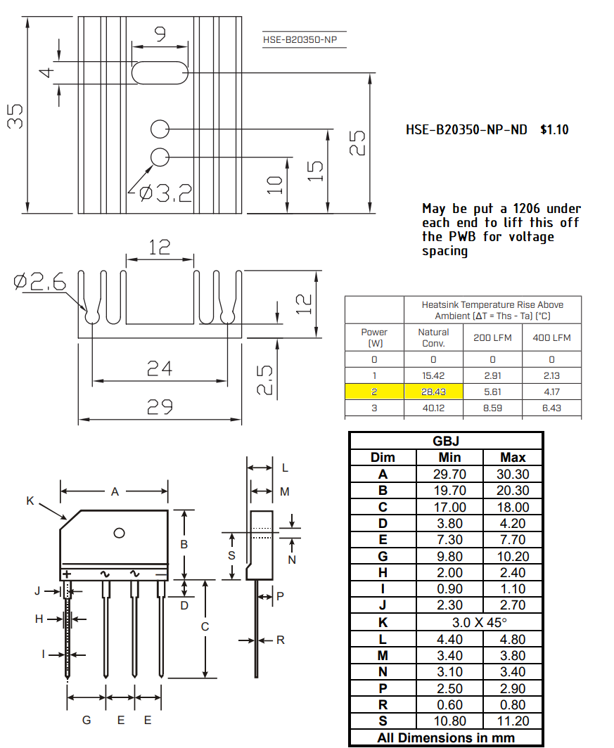
For the IGBTs, I'd probably use a Bergquist K10 SPK10-0.006-00-104 (Digikey/Mouser) for the thermal insulator. The insulator should be around 0.5 K/W resistance. I don't like the plain silicon rubber thermal pads because I've had issues with punctures and with tearing when using them. The inner Kapton layer in the K10 pad prevents this. Searching by low cost, less than 15K/W heatsinks, Digikey came up with the 2057-HSK-047-07-ND TO 247 heatsink for $2.51 that screws into the PWB for mechanical support and we can put two IGBTs on it. You have to have patience to put two parts through 1 screw, but you can do it.
At the mounting screws, I would put a split washer and flat washer between this heatsink and the PWB so that we could run traces under it by the IGBTs.
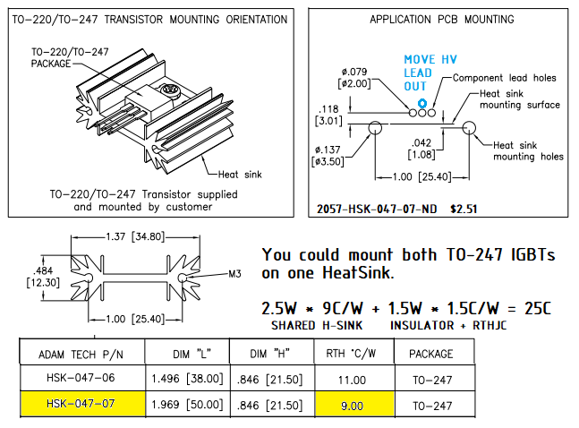
As an alternative, there is a 14C/W non-supported heatsink that could work on the diode pack or even with the IGBTs if the output power goes higher than 110W.
In my copy of LTSPICE, the LT1017 and LT1018 comparator models do not always switch low when they are supposed to switch low. I don't know if the latest update fixes this because I have problems running the LTSPICE update since I installed my latest Antivirus Software.
The Model for the IGBT shows it will conduct in reverse, like it had a diode from Drain to Source. Many IGBTs do not have an Co-Pak diode from Drain to Source and cannot be used for reverse conduction EVEN IF the model shows it conducts in reverse. This isn't LTSPICE's fault. It is in the Model itself. I added an external diode to perform this function. It is a standard recovery speed diode so that it has lower power loss. It should not need to ever switch fast.
The NPN and PNP transistor models do not have the Vbe and Vce breakdown voltages in the model. From what I was told (by a trustworthy source), the Vbe breakdown is a low voltage breakdown that damages the base-emitter junction. Vbe breakdown can make the part noisier and it really does reduce the current gain (Hfe). The Vce breakdown is a little more forgiving for you mainly have to worry about "hot spotting" on the die and smoking the part.
I have found on 3 computers, LTSPICE runs the fastest if you set the number of threads = Number of Cores - 1. On one computer it was almost twice as fast.
Sometimes a small change keeps the SPICE model from finding the DC operating point to start the transient simulation. If that happens, let LTSPICE run a bit
Gmin Stepping, wait for 100%, don't use ESC
1st Stepping Source, wait for first 99% or longer and hit ESC
2nd Stepping Source, wait for first 98% or longer and hit ESC
Pseudo-Transient Analysis wait for over ~50usec and hit ESC
If you spam the "ESC" key by hitting it like a Galaga Video Game Button, that can break the simulation and you have to start over. When it takes >30 minutes for some models to run, starting over isn't fun.
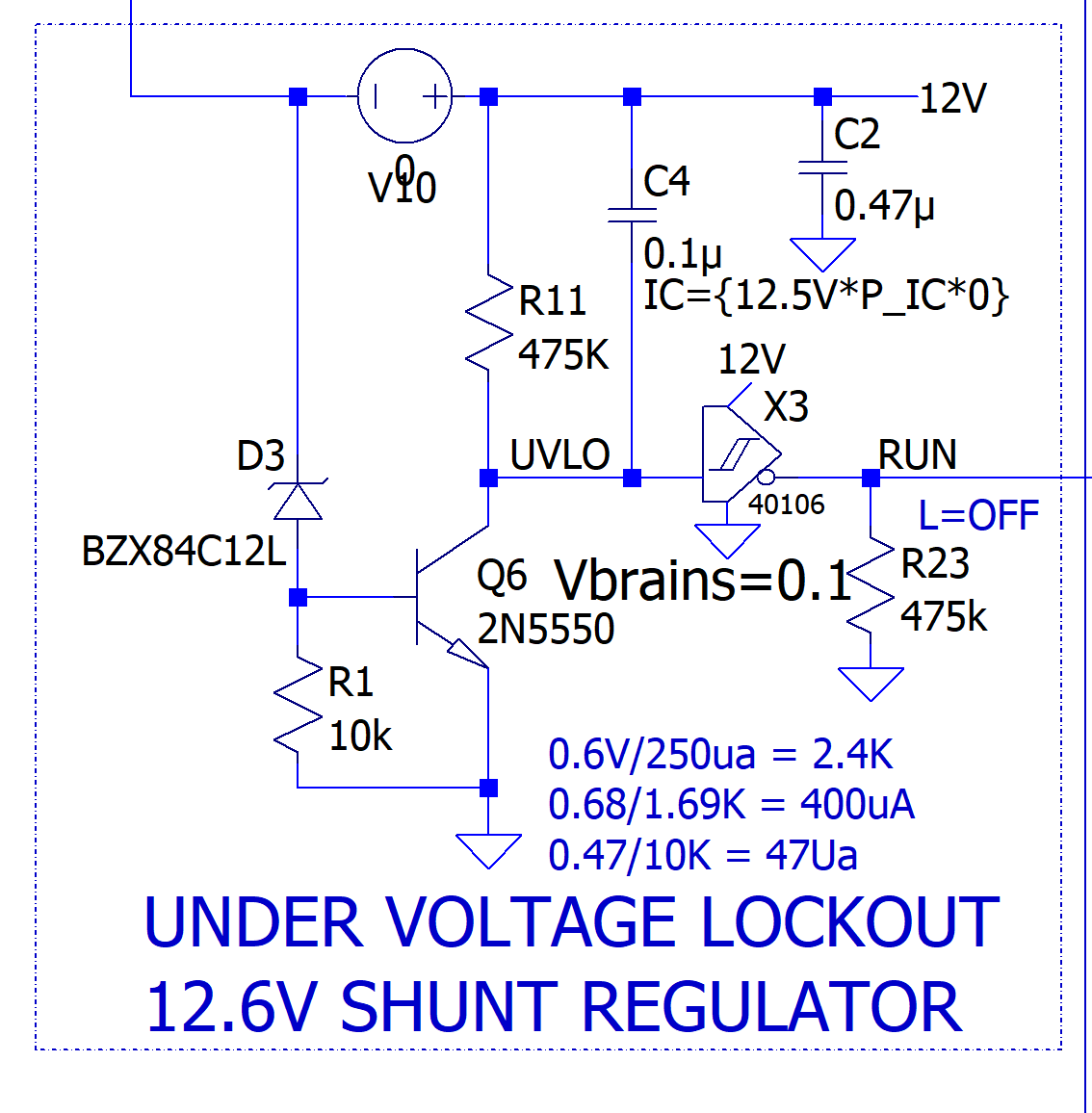
Make sure that when you build this that you use the LM2901B. Do not use the non-B version of the comparator. The "B" version only draws 1.6mA from the 12V rail. A 2.5mA Icc from the non-B model requires a redesign of the Rbias Circuits.
LM2901B / LM339B 1.6mA Icc 5.5mV offset from -40C to +85C
LM2901/LM2901AV 2.5mA Icc at 25C, 4mV offset -40C to +125C
I want that 0.9mA for the "B" version because it comes from the 108 to 132Vac Input. The LT1018 has a lower Icc, but it is a much slower device. I'll recommend we go for the speedier LM2901B.
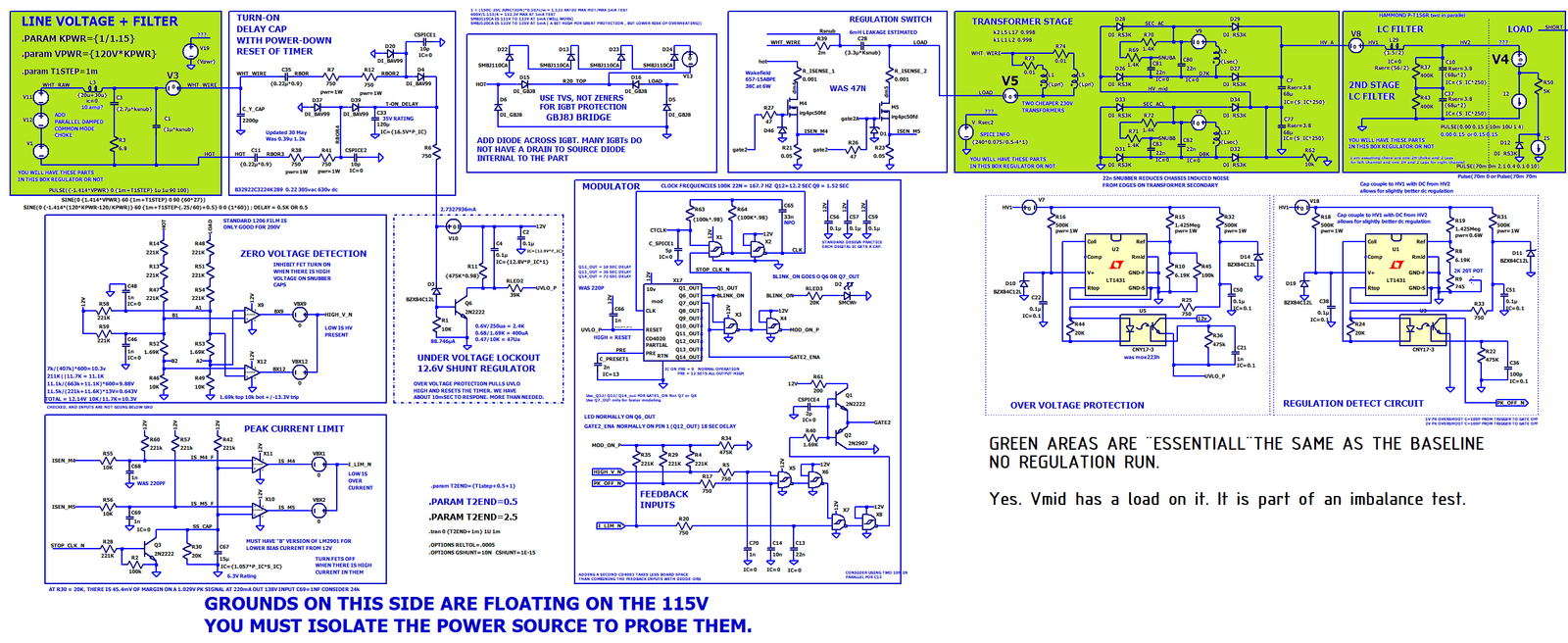
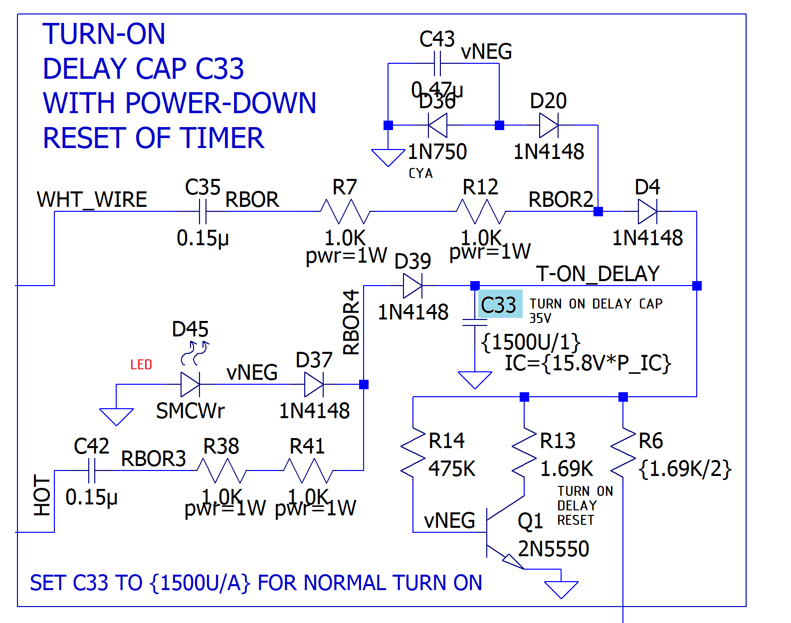
The floating 12V supply is generated with a charge pump. For modeling convenience, its ground is set to normal ground. In real life, the primary ground will float between the 115V rails. C11 and C35 provide the primary power. They prove enough to power start the circuit at 104V 60Hz without much margin. Making them 0.39uF increases the margin, but makes R7, R12, R38, R41 run hotter.
C33 only has to hold the power up for a bit more than 2 line cycles. 120uF is enough.
The 12V shunt regulator is shown below. To test it, put two 9V batteries across C33, the T-ON_DELAY cap. The current into the base of Q6 is critical. It keeps UVLO low which enables the primary side control electronics. It can do its job with 3uA, I prefer something closer to 300uA at low line. When the chopper starts, the ringing voltage on the 115V from the chopping action increases the current delivered by C11 and C35 above..
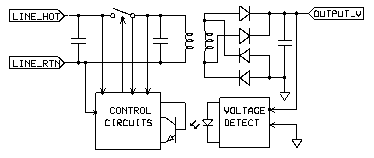
On an over voltage event, the circuit pulls UVLO_P high and resets the warm-up timer to time=0. This will keep the circuit from running in the over voltage condition.
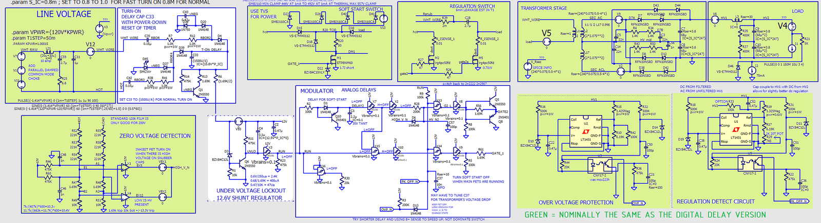
The digital controller is shown
below. The top half is the warm-up delay timer. The bottom half is the
feedback/chopper logic. I slowed the turn on the of IGBTs
with R61 to reduce the potential noise made from a high current turn
on pulse. R61 has to be "tuned" to the MOSFET being used, but it the
tuning is in 20% steps, not 1% value changes.
The "Blinky LED" blinks when the circuit is in the warm-up delay mode
and goes solid when the regulator is enabled. Each of the
feedback inputs has a different delay. That helps us tune up the
circuit for good operation. I would leave this LED on the controller's
circuit card. The leads on the LED will have a noisy 115V on it that
you don't want to run to front panel of your amp.
Your eyes are logarithmic just like your ears. If you want the LED to be "Twice as Bright", you need 8 to 10 times the power in it. So don't drop the value of RLED3.
This generates a low output when there is positive or
negative voltage between HOT and LOAD. The differential detection
circuit is more robust with detecting "zero voltage" in this location
than detecting that both Hot to Primary ground and Load to Primary
ground are both almost zero.
The comparator must be the "B" version of the LM2901B to limit the 12V
current draw. There are multiple manufactures of this part making life
easier for the hobbyist.
The LM2901B works from about -0.3V to Vcc-2V on its inputs. If one
input is inside the common mode range, the output transistor will be
in the correct state (On or OFF) At 25C, the upper common mode
limit is Vcc-1.5V.
Both A1 and B1 are pushing the 2V common mode voltage range, but B2 and A2 are not. Only one input has to be inside the common mode range for the LM2901B to work
The peak current limit's set resistor "R30" is mildly sensitive to the regulation of the power transformer used. Lower resistance (better regulation) in the transformer leads to higher peak currents in the IGBTs leading to needing to raise the ohms on R30
ISEN_M4 and ISEN_M5 can go below ground so R55 and R56 with R60 and R57 pull the voltage up to protect the comparator's inputs.
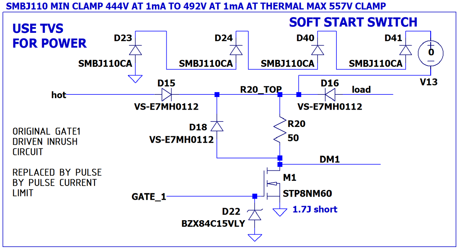
Under some load conditions, particularly at start up, there can be high voltage spikes that occur across the IGBTs. A bank of 4 TVS is used to clamp the peak voltage to a safe level. The two IGBT switches are diode-or'd to the TVS stack by the top diodes in a GBJ diode bridge. The bottom diodes in this bridge appear across the Drain to Source of the IGBT to control how negative the HOT and LOAD voltage goes below ground.
Unlike MOSFETs, IGBTs do not have an internal Drain to Source diode. We have to provide it. When current flows into "HOT" and through IGBT M4, the current tries to flow out to the "LOAD" through IGBT M5 in its reverse direction and it can't do it properly. D5 in the GBJ bridge completes this current path in the power switch circuit to provide power to the transformer. Likewise, D6 completes the current path when M5 is conducting.
We will want both the GB diodes and the IGBTs to have a low voltage drop at 20 amps peak.
Higher Voltage IGBTs, higher than the 600V one we are using, often have much higher voltage drops at 20 amps peak than the one shown below. We'll have to check the IGBT performance at 12V, not 15V.
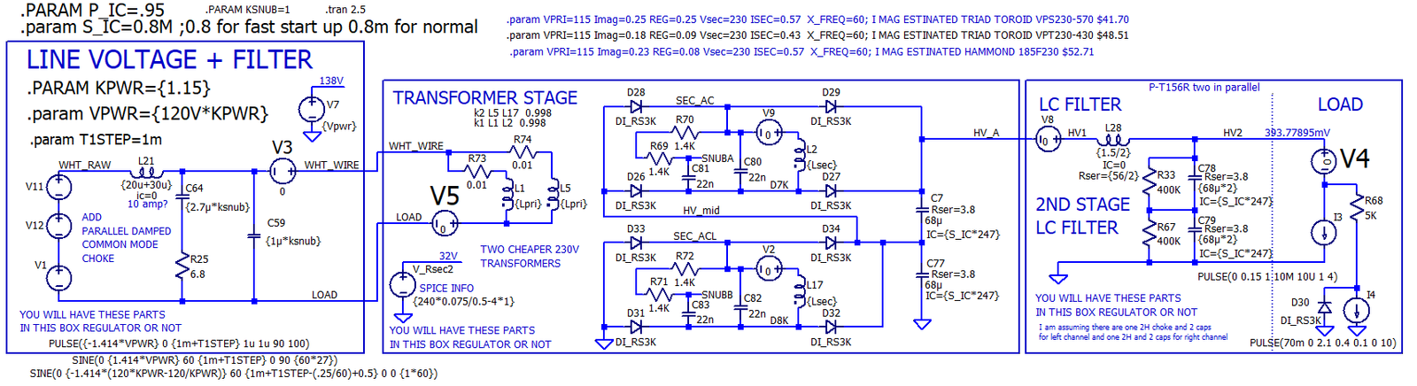
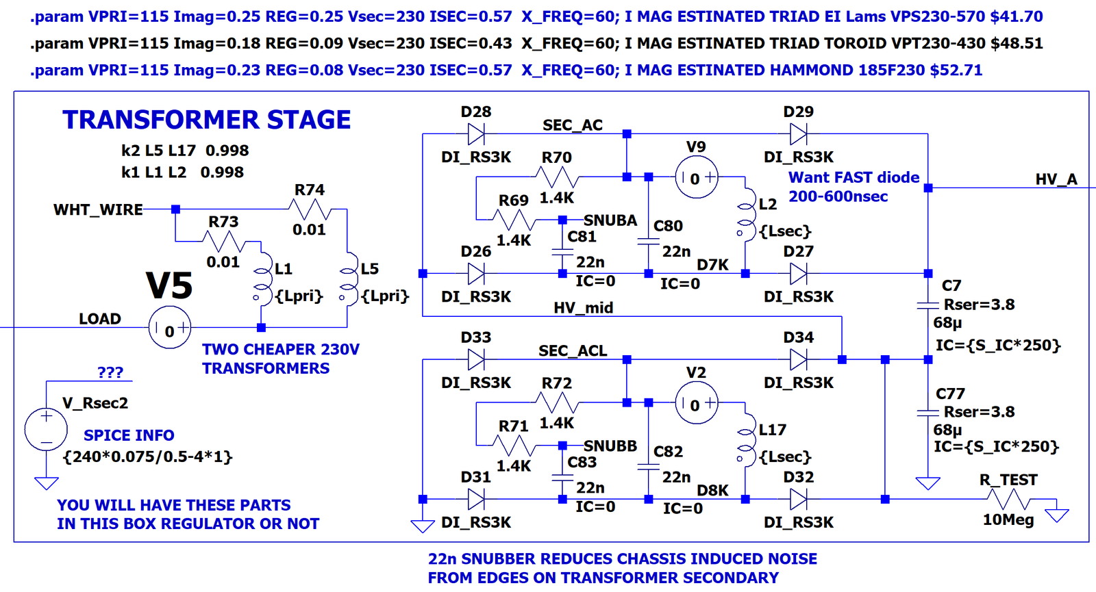
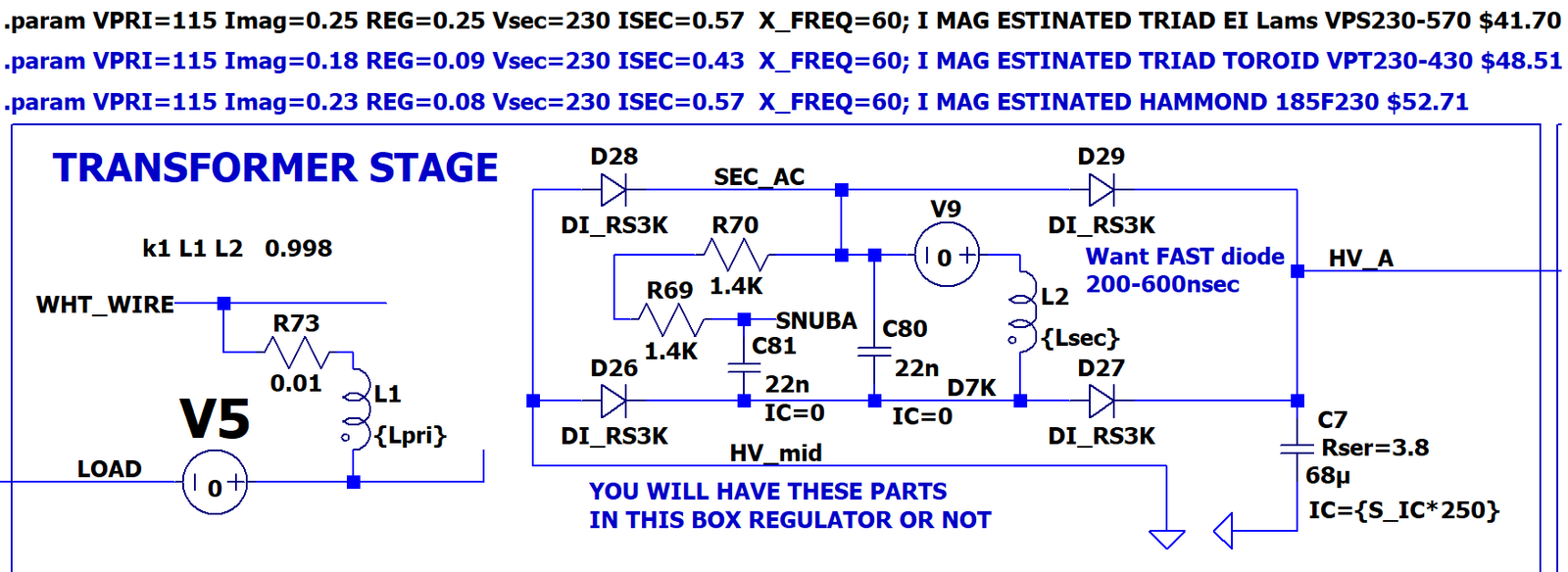
The transformer stage uses two standard 230V output transformers to make the 500Vdc. The primaries are in parallel. The secondaries are stacked "after" the diode full wave bridge.
I haven't tried many methods to stack the secondaries yet. I have run the model with an "imbalance" on the center tap (top of C77, HV_mid), on the one run I made, it behaved well. With the imbalance, the lower capacitor had about 3V less across it than the upper cap but the current pulses in V5 were well-balanced indicating that the circuit was behaving.
The connections below should work as a 4 diode instead of an 8 diode rectifier. I'd place the snubbers to connect to HV_MID so that the peak voltages are lower on the snubber parts.
I ran the models. I found that a voltage doubler does not work. The voltage doubler circuit can't maintain the balance between the voltages on C7 and C77. The peak output voltage is still contolled, but the output is noisy and the stresses higher and are not balanced on the parts.

The snubbers on the secondaries are highly recommended and are nearly a required part. When the primary switch turns off, the voltage on the secondary wants to move "FAST" and we want to keep it slow to hold the noise it generates down to a minimum. I normally want at least 30% margin on a film capacitor's AC voltage at high line. This makes the minimum AC rated voltage on the snubber capacitors >= V pk-pk / 2 / sqrt(2) / 0.7 = Vpkpk/2.
I have three transformer models set up. I had to estimate the Imag and coupling factor on each of them.
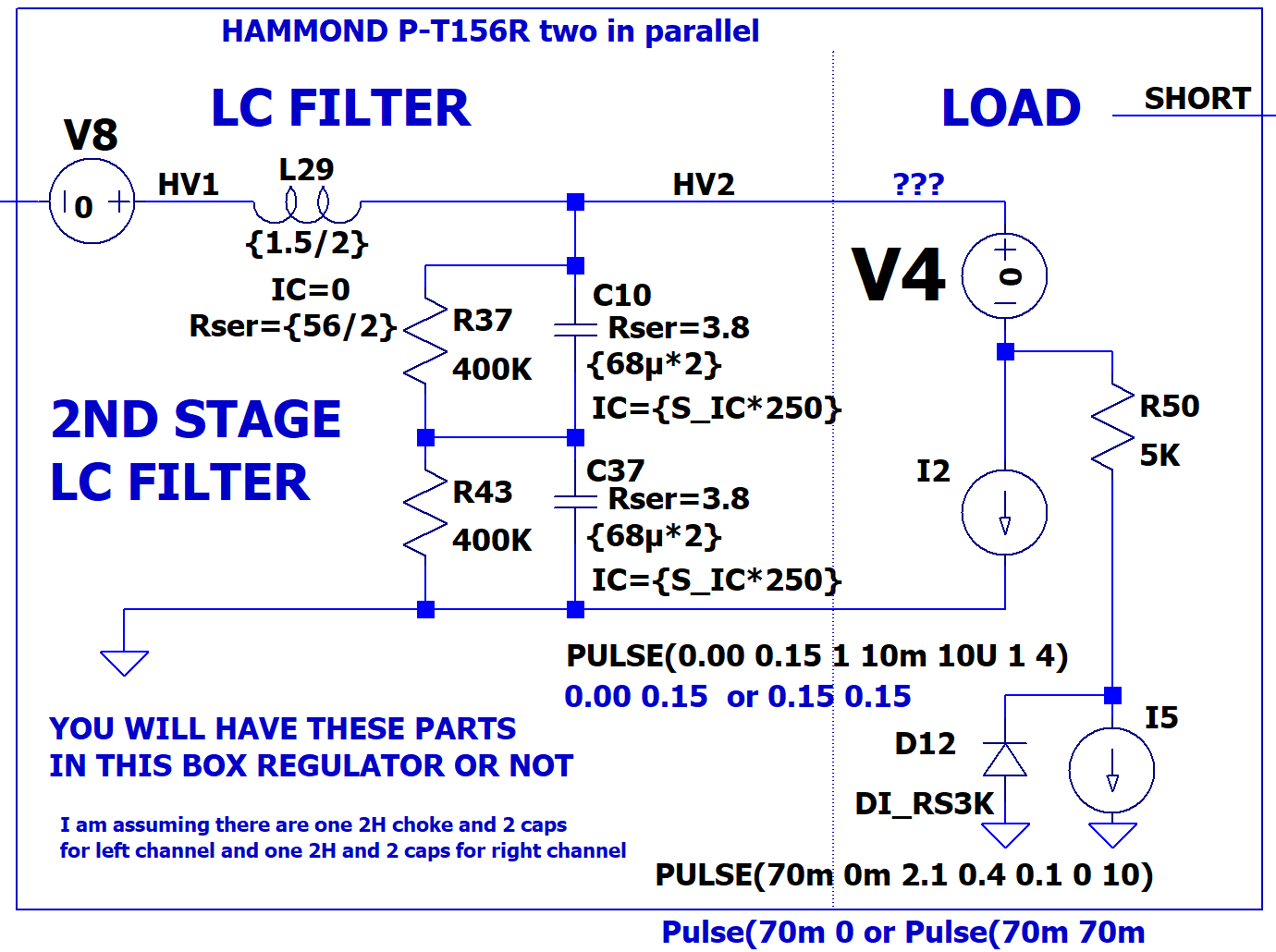
There should be an external LC filter attached to the first capacitor bank. This will limit the noise on the first bank from getting to the load. The non-zero output impedance of the first regulator stage help to damp the LC filter tank.
A 6V DC drop in the first capacitor for a 150mA load change makes the first stage output impedance 6V/0.15 = 40 ohms. The characteristic impedance of the LC tank is Zo = sqrt(L/C) = sqrt] (1.5H/2)/(68uF*2/2) ] = 105 ohm. The series Q of the LC filter is Zo/Rseries = 105 ohm/(40 ohm first stage +56 ohm DCR/2 parts) = 105/68 = 1.54. A "Q" of 1.5 is usually acceptable. Q total's over "2.0" can cause problems. Two old discussions on "Q" are located here LC Tank Q and Damping Ringing in LC tanks.
With a SET, it is possible to adjust the "tone" of your bass response by changing the "Q" of your power supply's LC filter. When the output LC tank goes resonant, the power supply's output impedance will increase and change the damping factor of your amplifier. You don't "have" to have a ruler flat frequency response. Make it sound the way you like it to sound. If "Mr. Snooty Ears" doesn't like it, he can build his own amp!
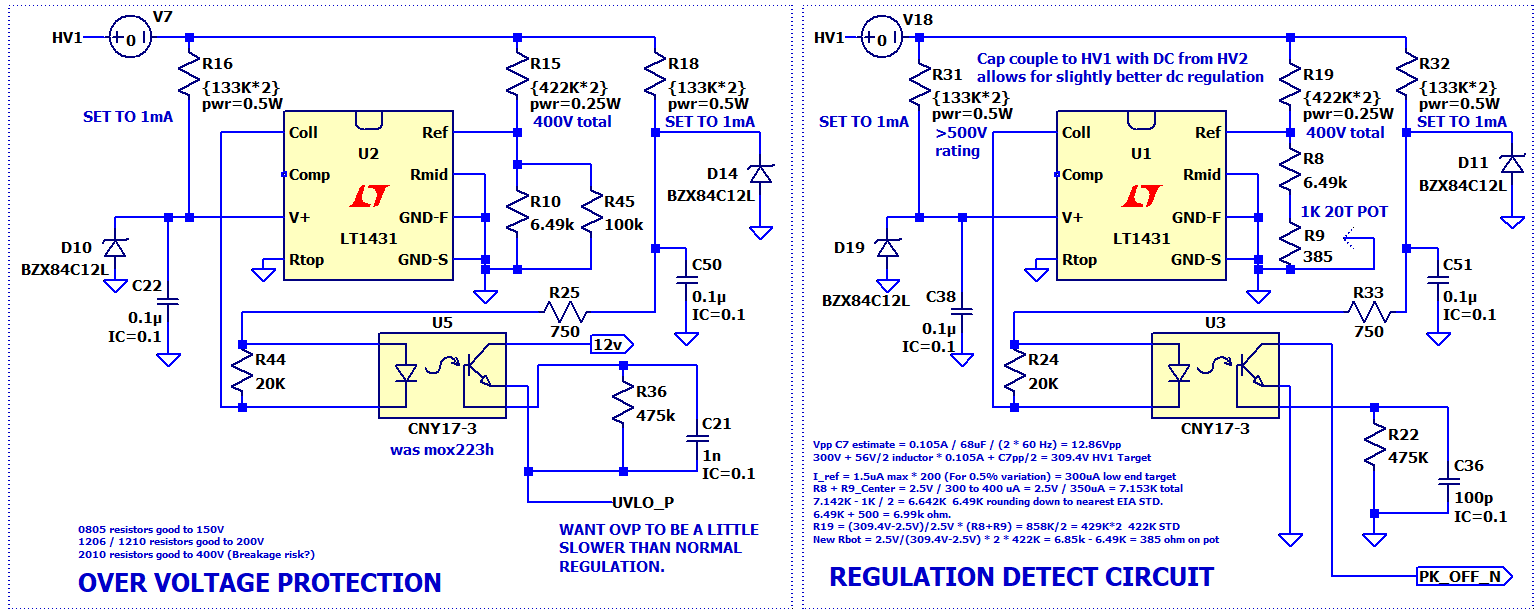
Some people will leave the Overvoltage Protection out of the circuit. I do not recommend it. If you turn the power on without tubes or with the filament supply disconnected, the output voltage could greatly rise if the main regulator path broke.
I had a system-lead accidentally short the power supply feedback resistors out by where he had placed the scope probe ground. He didn't like that the OVP circuit was tripping so he jumpered the OVP out instead of finding out why it was tripping. He proceeded to destroy several thousand dollars worth of boards. For some reason, it was my fault. . . If your system can handle the high no load voltage with the regulator shorted out for days on end without it being a fire hazard or destroying $$$ in tubes, you can take the OVP out. I'm leaving it in.
Most of us will want to tweak the DC output voltage, so I provisioned for a 20 turn pot to do a fine adjustment. It is presently set for 7V (1.3%) per turn on the POT in this example. We could change to a 1K pot, recenter R8 and R10 and get a finer voltage adjust range.
In the 300V 105mA example below, I go over picking resistor values for this section.
I would try for 5mm creepage on the PWB for the opto-coupler's input to output.
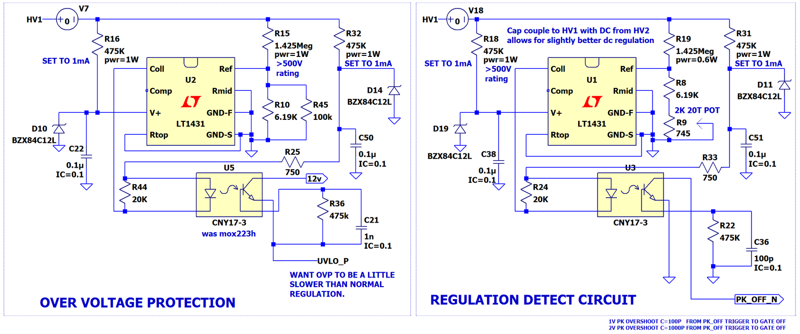
Watch the voltage spacing in your
layout. This goes beyond maintaining the 4 to 5mm safety creepage.
Example:
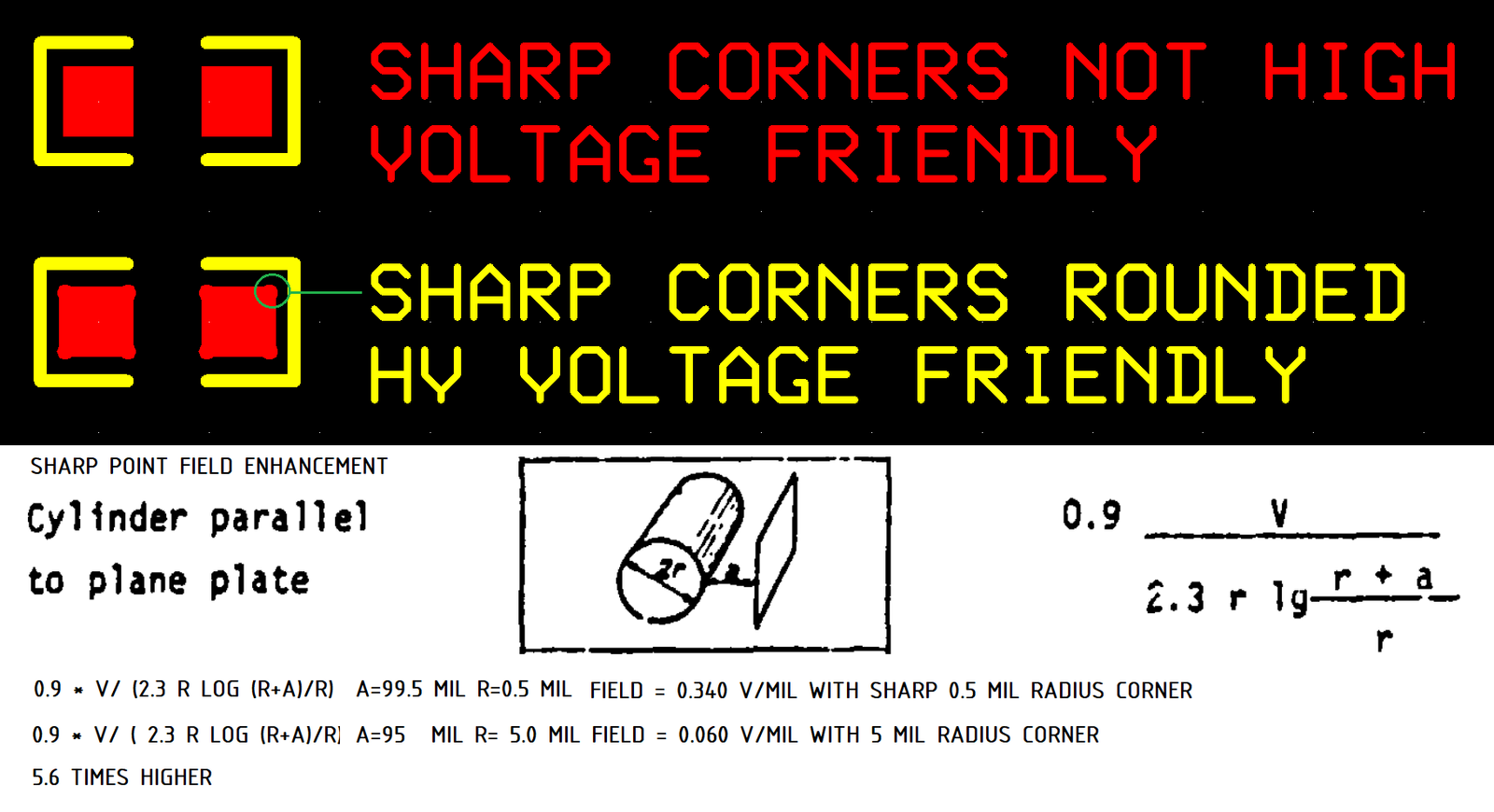
I was planning on making the 1.425megohm R19 out of three series 475K 1% 100ppm/C 200Vdc thin film resistors. The spacing between lands should be 98.4 mils (2.5mm) with the corners on the lands rounded off by a 5 mil radius copper circle. The voltage breakdown difference in rounding off the corners can be measured in real life, it isn't just scratches of math on a paper.
Note: "Lg" in the formula is log base 10, not "ln" the natural log. The 2.3 in the denominator of the equation turns a Log base 10 into a natural log (ln). This formula is from AFWAL-TR-88-4143 Vol II Table 19 page 135.
With the warm-up timer set to use Q12_OUT, we get a 19-second turn on delay. 18.4 seconds of the delay is from the digital timer. This plot was taken at 104Vac input. The LED blinking on and off has a noticeable impact on the base current of Q6 (the UVLO detector).
Don't make the LED use more current if you don't also change Cbias and Rbias.
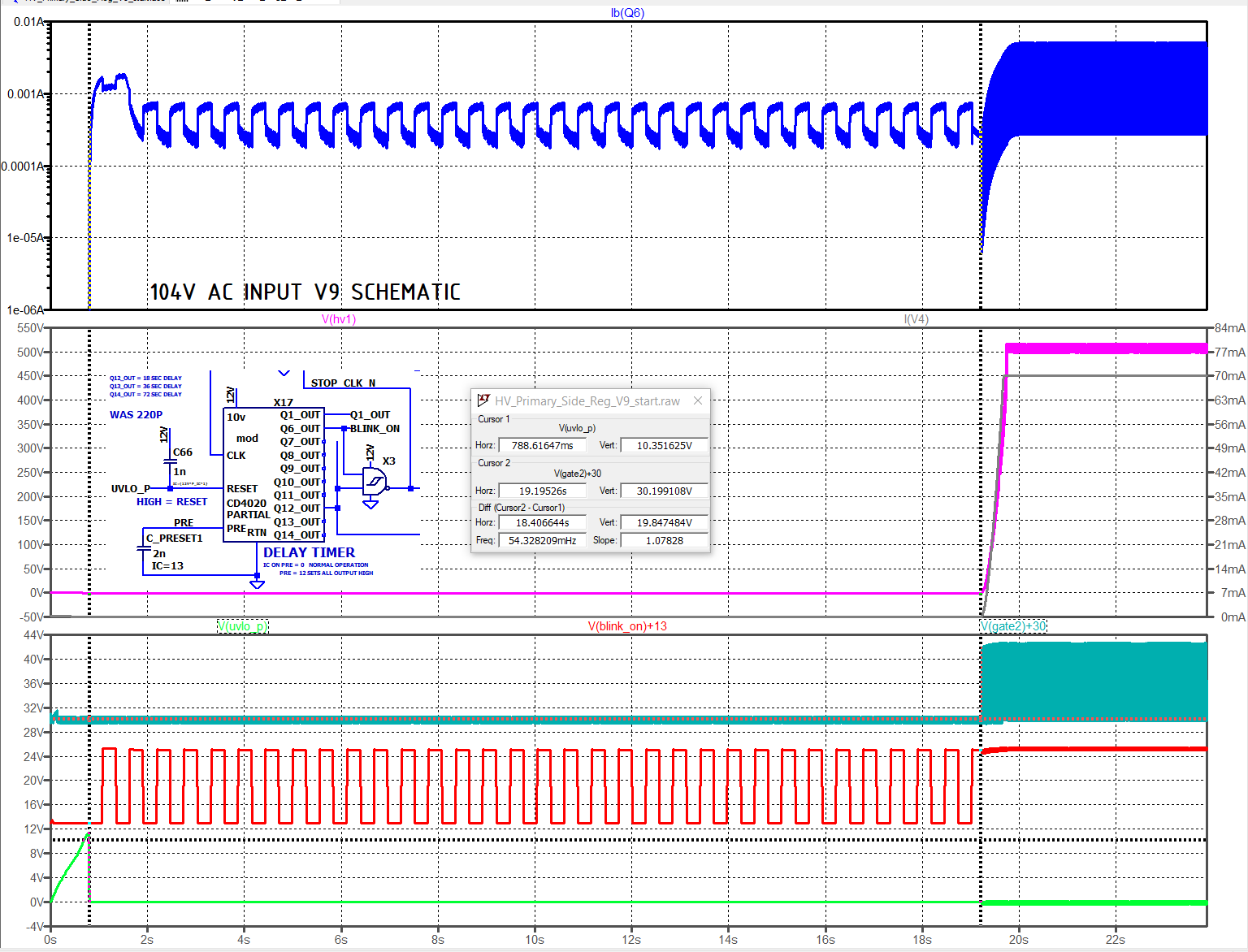
Zooming in shows that Ib(q6) looks good.
The primary inductance is estimate from Lpri = (115V Test Voltage/ I_mag) / ( 2 PI 60Hz) from data sheet. This lumps the core loss in with the magnetization current, this is an error, but it is the best we can do with the datasheets we get. If your datasheet doesn't list I_max (excitation current), look for a similar weight part in the Hammond Audio Power Transformer line. Toroidal transformers tend to have a lower Imag than EI lamination designs.
The secondary inductance is equal to Lpri * [ (Vsecondary * (1+regulation)) / Vprimary ] **2 ( **2 = squared, SPICE was written in FORTRAN," ** "is used to raise something to a power in FORTRAN, not " ^ " like in EXCEL.)
For 60 Hz transformers, a coupling factor of 0.998 is reasonable. Again, I wish for better data from the data sheets.
k = sqrt(1 - Primary Side Leakage Inductance/Primary Inductance)
If the data sheet gives the primary and secondary DC resistance, just use it. If not
Rsecondary = Vsecondary * % regulation / I rated Secondary / 2 The "/2" is because normally half the regulation loss is in the primary and half in the secondary.
Rprimary = Vprimary * % regulation / I rated primary (not counting magnetization current) / 2. The "/2" is because normally half the regulation loss is in the primary and half in the secondary. OR more easily
Rprimary = Rsecondary * Lpri/Lsec
I need a 300V 95mA B+ for a design where I'm going to push the power in the output tube. Since Phoenix has a wide range of power quality on the 120V (105Vac to 135Vac), I want the output to be regulated, so that my amp works the same at my house as it will at my buddy's house. I'm going to add 10% more to the current and plan for 105mA. Let us see what we get with the 9% regulation transformer, and what can we get with the 25% regulation transformer?
To set the filtered output voltage to 300V, we will need to know the line frequency (60Hz), the output capacitance (C7, 68uF), the load current (105mA) and the DCR of the LC filter (56 ohm/2 in parallel (Left and Right channel)).
First calculated the estimated ripple on the output capacitor
Vpp C7 estimate = 0.105A / 68uF / (2 * 60 Hz) = 12.86Vpp
Then raise the regulation peak point by half the peak to peak ripple, plus the IR drop in the inductor.
300V + 56V/2 inductor * 0.105A + V(C7)pp/2 = 309.4V HV1 Target
Pick the resistive divider's bias current to be 200 times the input bias current of the LT1431. 200X gives us approximately a 0.5% error in the voltage from the reference current.
I_ref = 1.5uA max. 1.5uA * 200 (for 0.5% variation) = 300uA
low end target in resistors
R8 + R9_Center = 2.5V / 300 to 400 uA = 2.5V / 350uA = 7.153K total
The adjustment pot should be about 10% to 30% of this target resistance or 700 to 2130 ohms. Let us use a 1K 20 turn pot. Let's pick R8 with the pot set to center and then round to a standard resistor value for R8.
7.142K - 1K / 2 = 6.642K Rounding down, 6.49K is the
nearest EIA Standard value.
6.49K + 500 = 6.99k ohm. <- R8 + R9 total
Now we pick the top resistor value. A 300V rail will require two 200V resistor in series.
R19 = (309.4V-2.5V)/2.5V * (R8+R9) = 858K/2 = 429K*2 Use two 422K Standard value parts in series.
150V^2 / 422K = 53mW in the resistor, which will work on a 1/4W resistor. Because this is a reference divider, we really want more than 2:1 power derating. We have nearly 5:1 derating, so the design is good.
Lastly, adjust the pot for 309.4V peak on HV1. We adjust the pot because we used real world values for the resistors, not the exact values we calculated.
New Rbot = 2.5V/(309.4V-2.5V) * 2 * 422K = 6.85k needed - 6.49K in R8 = 385 ohms on the pot
300V/6.85K = 0.4817V/ohm * 1Kohm/20T = 2.19V/Turn on the adjustment pot. With +/-1/8 turn being feasible on the pot a +/-0.27V output setting is possible.
The bias resistors for V+ and the LED should conduct at least 1mA.
(309V-12V)/1mA = 297K 297K/2 = 148K max for 2 resistors in series. 150^2/148K = 0.151W (Acceptable on a 1/4W part). 154V^2/ 0.25W / 0.75 margin = 126K, round up to 133K (because I have some already)
(309-12V) / (2 * 133K) = 1.118mA which is more than 1mA, so the design is good.
For the OVP, I use the same parts, but I short out the POT and place a trim resistor across R10 that is 10 to 20 times R10..
The current limit resistors were changed from 0.05 ohms to 0.10 ohms because the output power is about 1/3 that of the 500V 0.22A 110W design. The current reference voltage stayed the same and was made with a 20K ohm 221K to the 12V rail.
For simplicity, I just took one of the two transformers in the 500V design out.
The changes to the OVP and controller are as shown. I'd use a stack of resistors whose total is rated for 400V going to the HV. The "V+" needs at least 1mA of bias and the LED needs 1mA too.
9% regulation transformer doesn't have enough voltage from the secondary to deliver 300Vdc regulated at low line input. It drops out at 109Vac input.
If we are desperate, we could set the regulation point to be 289V/estimated 1.03= 280Vdc to use the 9% transformer.
:-) :-) :-)
The 25% regulation 0.57A transformer can deliver 300Vdc regulated at HV2. With the regulator set to almost the over voltage trip point, the model predicted we would get 321Vdc out with 106Vac input. 321V/1.03% tolerances = 311Vdc is possible on HV2 if we use the 25% regulation transformer. This higher voltage is because the unloaded 230V secondary will run 25% high and the resistance of the winding are set for a 25% drop at 0.57Arms to pull the output into regulation. 0.57A is more current than we need, but the higher current rating is one of the things that allows this transformer to work in our circuit.
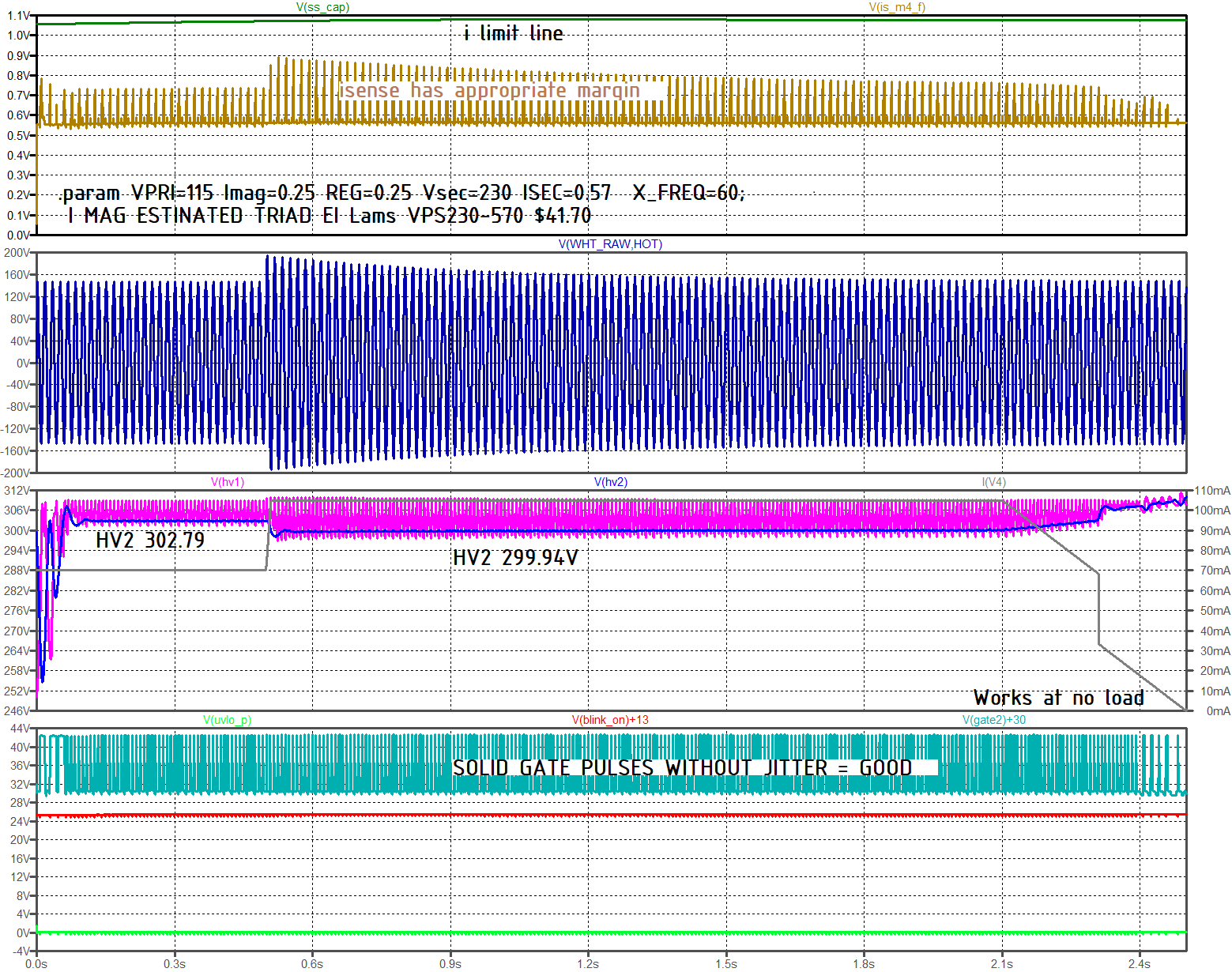
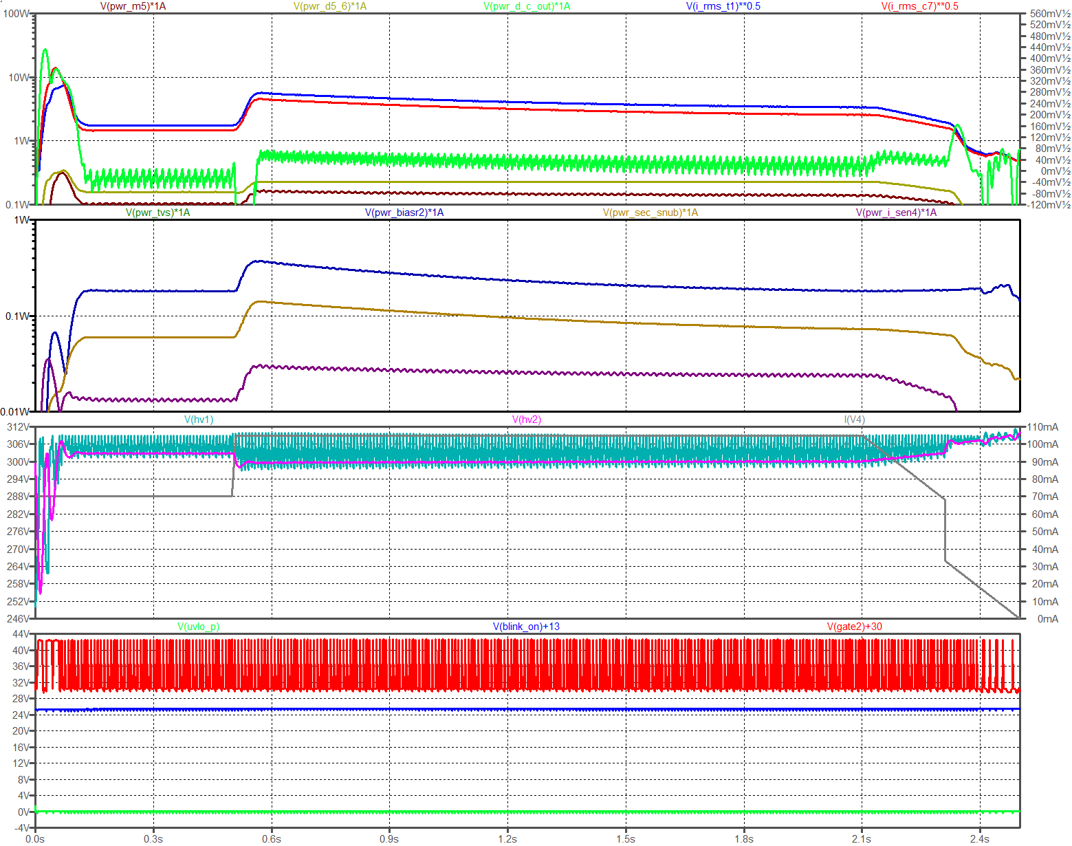
The 300V 105mA power losses are lower than on the 500V 0.22A design. The 25% dynamic plots are below. Examine the .meas data below for values..
a_i_ibq6_min_____:
MIN(Ib(Q6))=0.000380397395929 FROM 0.631165665764 TO 0.647832332387
a_i_load_v4______: AVG(I(V4))=0.1050037432 FROM 0.631165665764 TO
0.647832332387
a_i_r6___________: AVG(I(R6))=0.00865417277127 FROM 0.631165665764 TO
0.647832332387
a_irms_c7________: AVG(V(I_RMS_C7)**0.5)=0.250042656641 FROM
0.631165665764 TO 0.647832332387 < -- 0.25A in the
output capacitor is good.
a_irms_input_____: AVG(V(I_RMS_INPUT)**0.5)=0.81933400436 FROM
0.631165665764 TO 0.647832332387
a_irms_t1________: AVG(V(I_RMS_T1)**0.5)=0.271828684124 FROM
0.631165665764 TO 0.647832332387 < -- 0.27A on a 0.57A
transformer is good.
a_p1_t1__________: AVG(V(PWR_T1))=7.65029837591 FROM 0.631165665764 TO
0.647832332387
a_p2_p_d_c_out___: AVG(V(PWR_D_C_OUT))=0.57214912156 FROM
0.631165665764 TO 0.647832332387
a_p3_ctrl________: AVG(V(PWR_CONTROLLER))=0.523403155957 FROM
0.631165665764 TO 0.647832332387
a_p4_m4__________: AVG(V(PWR_M4))=0.171733355989 FROM 0.631165665764
TO 0.647832332387
a_p4_m5__________: AVG(V(PWR_M5))=0.160329944677 FROM 0.631165665764
TO 0.647832332387
a_p6_d5_6________: AVG(V(PWR_D5_6))=0.225676930373 FROM 0.631165665764
TO 0.647832332387
a_p7_biasr2______: AVG(V(PWR_BIASR2))=0.343726295828 FROM
0.631165665764 TO 0.647832332387
a_p8_biasr_______: AVG(V(PWR_BIASR))=0.346008520687 FROM
0.631165665764 TO 0.647832332387
a_p9_0_p_zero_det: AVG(V(PWR_Zero))=0.0610246630417 FROM
0.631165665764 TO 0.647832332387
a_p9_1_p_i_sen5__: AVG(V(PWR_I_SEN5))=0.0256750732149 FROM
0.631165665764 TO 0.647832332387
a_p9_2_p_12v_drv_: AVG(V(PWR_12V_DRV))=0.166139508256 FROM
0.631165665764 TO 0.647832332387
a_p9_3_p_tvs_____: AVG(V(PWR_TVS))=0.00290486933852 FROM
0.631165665764 TO 0.647832332387
a_pin____________: AVG(V(PWR_IN))=43.2181139626 FROM 0.631165665764 TO
0.647832332387
a_pout___________: AVG(V(PWR_OUT))=33.4382901089 FROM 0.631165665764
TO 0.647832332387
a_pwr_loss_______: AVG(V(PWR_LOSS))=9.77982384458 FROM 0.631165665764
TO 0.647832332387
a_pwr_sec_snub___: AVG(V(PWR_SEC_SNUB))=0.133535048215 FROM
0.631165665764 TO 0.647832332387
a_r20____________: AVG(V(PWR_R20))=0 FROM 0.631165665764 TO
0.647832332387
a_r39____________: AVG(V(PWR_R39))=0.000319882195657 FROM
0.631165665764 TO 0.647832332387
a_vhv1_avg_______: AVG(V(HV1))=302.631356812 FROM 0.631165665764 TO
0.647832332387
a_vhv2_avg_______: AVG(V(HV2))=299.678623564 FROM 0.631165665764 TO
0.647832332387 <--- 0.1% off target is really good.
This data is from the 0.6 second point where it is regulating.
a_i_ibq6_min_____:
MIN(Ib(Q6))=0.000258541665971 FROM 0.631165597445 TO 0.647832264229
a_i_load_v4______: AVG(I(V4))=0.105003739256 FROM 0.631165597445 TO
0.647832264229
a_i_r6___________: AVG(I(R6))=0.00755371979835 FROM 0.631165597445 TO
0.647832264229
a_irms_c7________: AVG(V(I_RMS_C7)**0.5)=0.267164366761 FROM
0.631165597445 TO 0.647832264229
a_irms_input_____: AVG(V(I_RMS_INPUT)**0.5)=0.71246514395 FROM
0.631165597445 TO 0.647832264229
a_irms_t1________: AVG(V(I_RMS_T1)**0.5)=0.2872666315 FROM
0.631165597445 TO 0.647832264229 <-- 0.287A on a 0.43A
transformer (good)
a_p1_t1__________: AVG(V(PWR_T1))=4.48669851274 FROM 0.631165597445 TO
0.647832264229 The 25% regulation transformer had
7.65W of loss
a_p2_p_d_c_out___: AVG(V(PWR_D_C_OUT))=0.61317377438 FROM
0.631165597445 TO 0.647832264229
a_p3_ctrl________: AVG(V(PWR_CONTROLLER))=0.47478890481 FROM
0.631165597445 TO 0.647832264229
a_p4_m4__________: AVG(V(PWR_M4))=0.146458506589 FROM 0.631165597445
TO 0.647832264229
a_p4_m5__________: AVG(V(PWR_M5))=0.139110366802 FROM 0.631165597445
TO 0.647832264229
a_p6_d5_6________: AVG(V(PWR_D5_6))=0.191113266737 FROM 0.631165597445
TO 0.647832264229
a_p7_biasr2______: AVG(V(PWR_BIASR2))=0.309904870823 FROM
0.631165597445 TO 0.647832264229
a_p8_biasr_______: AVG(V(PWR_BIASR))=0.346383259172 FROM
0.631165597445 TO 0.647832264229
a_p9_0_p_zero_det: AVG(V(PWR_Zero))=0.0556184592934 FROM
0.631165597445 TO 0.647832264229
a_p9_1_p_i_sen5__: AVG(V(PWR_I_SEN5))=0.0193711611562 FROM
0.631165597445 TO 0.647832264229
a_p9_2_p_12v_drv_: AVG(V(PWR_12V_DRV))=0.131011784807 FROM
0.631165597445 TO 0.647832264229
a_p9_3_p_tvs_____: AVG(V(PWR_TVS))=0.00268606849005 FROM
0.631165597445 TO 0.647832264229
a_pin____________: AVG(V(PWR_IN))=39.9100876833 FROM 0.631165597445 TO
0.647832264229
a_pout___________: AVG(V(PWR_OUT))=33.402792977 FROM 0.631165597445 TO
0.647832264229
a_pwr_loss_______: AVG(V(PWR_LOSS))=6.50729470197 FROM 0.631165597445
TO 0.647832264229
a_pwr_sec_snub___: AVG(V(PWR_SEC_SNUB))=0.148533823178 FROM
0.631165597445 TO 0.647832264229
a_r20____________: AVG(V(PWR_R20))=0 FROM 0.631165597445 TO
0.647832264229
a_r39____________: AVG(V(PWR_R39))=0.000305440746956 FROM
0.631165597445 TO 0.647832264229
a_vhv1_avg_______: AVG(V(HV1))=302.384701448 FROM 0.631165597445 TO
0.647832264229
a_vhv2_avg_______: AVG(V(HV2))=299.432826537 FROM 0.631165597445 TO
0.647832264229
This version uses an analog delay similar to the one used on The Clap-R Secondary Side Regulator. The Primary Side Power Supply, the UVLO and the Modulator are different than what was shown in the digital delay control circuit, the other sections of the circuit stayed the same (other than any last minute tweaks). I prefer the digital delay version to this one. I started the analog delay design first and have already spent weeks getting the analog version to work so I felt the need to share it. The digital delay circuit uses a turn on delay timer similar to the one in HV_RECT_SEC_SIDE EZ80 REPLACEMENT.
In the first versions of the zero voltage crossing circuit I tried to use the voltage from "HOT" and "LOAD" to primary ground to determine the zero voltage switch point. This did not work. There was an inconsistent low frequency ripple on the high voltage output. To fix this I added a LM139 zero crossing detector. The 2.7uF (3.3uF) snubber used to be from "HOT" to "LOAD" and it also did not work as good as having it across the primary of the transformer and a second cap placed across the power from the wall socket.
The LM139 (LM393 dual) is an old, but trustworthy comparator. The inputs will work to almost 0.3V below ground (Vee) and if one input goes above the voltage rail and if the other input is inside the common mode range, the output will go the correct state. One down side to this part is that it has a relatively high current draw from the voltage rail when compared to newer comparators. This extra current draw required me to provide more current from the primary side supply which may cause C33, the 11 second delay capacitor, to need to grow larger. The LM2901B is a lower current version of this comparator and will solve some of these issues.
The digital section shown above is a more updated design than the digital sections shown in green in the schematic below. I would build the newest digital design, not the analog one.
The current for the primary side regulator comes from a charge pump made by C35 and C42. When the circuit starts to "chop" the input voltage, the ringing on "HOT" and "LOAD" cause the current from these two capacitors to increase. But before that happens, C35 and C42 much charge up the turn on delay capacitor C33. As the leakage current from the parts on the board change (both from part to part and with temperature) and the 120V input changes, the amount of current available to charge C33 will change. This change will change the turn-on delay.
There is a turn on delay reset circuit in this section made with Q1, R13 and R14. During normal operation Vneg holds Q1 off. We have to be careful of the 5 Vbe breakdown voltage of Q1. I added a zener for extra protection should the LED fail open. When the 120V is turned off, Vneg decays and Q1 turns on which discharges warm-up delay capacitor C33. The Vneg also lights up an LED to let us know we have power.
The analog UVLO circuit adds an inverter to the UVLO output so that the "RUN" command snaps on and off. Without this buffered "Snap on-off" action, the inrush delay circuit won't work reliably.
The Base Current in Q6 lets us know how much margin we have in the current from the input charge pump. I normally like R1 to be closer to 2.4K, but I needed to starve R1's current for additional low line operating margin, The minimum current into the base is 13V/475K / 10 Hfe saturated = 2.7uA (3 uA).
R23 is a bleed resistor for "RUN' so that with the power off, the inrush duration cap is held close to zero and the other control ICs see a logic "zero".
The digital modulator has one more IC, the counter IC, than the analog modulator. This added IC in the digital version provides both a turn on warmup delay and a soft-start duration that is independent of the line voltage and temperature. With the analog version, line voltage and part leakage currents will change both the turn on warm up delay time and the soft-start charging duration. With the digital delay, there is an added bonus is that delay time can be easily changed from 18, 36 or 72 seconds by moving a soldered in jumper to choose a different tap on the counter IC.
When either the PK_OFF_N or OVP_N opto-couplers turn on, both Gate_1 and Gate_2 are turned off. C37 adds a pulse stretching action to keep the gates off for a short time after the optocouplers turn off.
C1 set the soft-start delay (Delay2). When C1 is low, Gate2 is off and Gate1 is on. When C1 is high, Gate2 is on and Gate1 is off.
When the gates are switched off, leakage inductance and primary inductance of the transformer will cause the voltage between "HOT" and "Load" to rise. When this happens, the zero voltage detection circuit pulls HIGH_V_N low keeping Gate_2 off, but not impacting Gate_1. High_V_N stays low until the sensed voltage decays to a safe level. Until the high voltage output is fully charged up, there will be enough voltage across the inrush limiting resistor to cause HIGH_V_N to trip, if it does, we want to keep Gate_1 on. Because of this, GATE1 ignores HIGH_V_N.
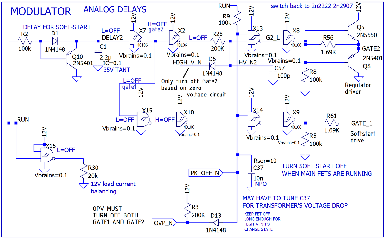
The original inrush circuit switched in a power resistor to soft-start the high voltage output. After seeing that the circuit would work into a short with pulse-by-pulse current limiting. I decided to change to use the pulse-by-pulse current limiter to soft-start the output voltage. All I had to do was slowly raise the current limit on this circuit from zero to full current.
The turn on plots shown below are with C33 set to 150uF and pre-charged to just below its normal operating voltage. With the inrush delay capacitor at its nominal value, with a nominal input voltage, the turn on delay is 16.3 seconds. This test was run with all part's leakage currents at maximum (i.e. set for a hot board.) At low input line this will be a longer delay. With a room temperature board, the delay also will also be longer. At high line, the delay will be shorter.
The Soft-start on the HV output shows an exponential voltage rise. This is from a 50 ohm on the primary side of the transformer charging up the output capacitors.
When the main regulating FETs turn on, the currents are higher than normal for the first few switching cycles. During this time, the TVS clamps the primary side "HOT" and "LOAD" voltages to protect the IGBTs and MOSFET. Make sure you use TVS for this function and not standard zeners.
During the simulation I watch the base current of Q6 closely. When it drops to zero, the UVLO goes high and shuts the regulator off. The base current of Q6 needs margin at low line turn on. The turn on below is at high line..
This simulation run starts with 138Vac input and has a dip down to 104Vac input.
A load change (at high line) of 70mA to 220mA causes a 14V dip in the filtered high Voltage Output. A step in line voltage from 138Vrms to 104Vrms gives a 6V change in the output voltage.
Without the fancier feedback as shown below:
High Line to Low Line 6.17V (1.2% of 500V)
70mA to 220mA Load 14.5V (2.9% of 500V)
In the 14V change for the 150mA load change, 4.5V of that change is from the DCR of the inductor in the LC tank.
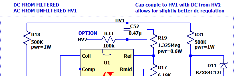
There is a "risky" option to pull the DC regulation from HV2. It is risky because the feedback includes the output LC tank (stability) and it has another sense "WIRE" (not trace) in the feedback loop (damage from fat-fingering something.)
With the fancier feedback shown above:
High Line to Low Line 6.71V ( No real change)
70mA to 220mA Load 11.65V ( A 3.0V improvement)
Notice that the ringing at 0.1 seconds of HV2 is slightly worse.
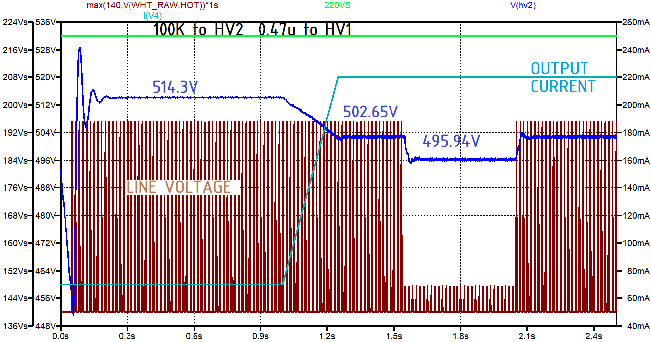
For the small improvement this change gives, I would use it. If the IR (current times resistance) drop in the output inductor were 20V instead of 4V, I'd consider it.
At an output voltage of 500V at 220mA, the primary part of the control card dissipates 3.41W stead state high line. The two MOSFETs that do the switching will need a small < 20C/W heatsink. The inrush MOSFET will need to have a little thermal mass added to it to support turn-on,. You can use either a small heatsink or a few steel washers in contact with the exposed metal on M1 to provide this mass.
The primary side losses are listed below (1.4% error in the totals = good enough).
|
|
Analog mW |
|
|
PWR_CTRL |
3.4080 |
< -- Total |
|
|
|
|
|
M1 |
0.0004 |
|
|
M4 |
0.9731 |
0.22A at 500V |
|
M5 |
0.9808 |
0.22A at 500V |
|
R20 |
0.0000 |
|
|
R39 |
0.0018 |
|
|
BiasR |
0.5419 |
|
|
BiasR2 |
0.5436 |
|
|
PWR_TVS |
0.0055 |
|
|
Primary
side Circuit power |
0.1370 |
IC’S ON 12V |
|
Zero V resistors |
0.0670 |
|
|
LED PWR |
0.0797 |
|
|
Isense |
0.0822 |
|
|
|
|
mA on 12 |
|
Missing |
-0.0051 |
-0.0004 |
|
|
|
|
|
Irms T1 sec |
0.5106 |
0.22A at 500V |
|
Irms C7 |
0.4676 |
0.22A at 500V |
|
Power 22nF |
0.5044 |
|
|
Power 22nF |
0.3905 |
|
|
Ib Q6 |
0.0054 |
|
|
I_R6 |
0.0071 |
|
With the given HV capacitive loading and turning on with a 1/3 full load present, R20 sees 19.2J of transient energy. Metal Oxide Film leaded resistors have a test rating for 6.25X rated power for 5 seconds or about 30J. We don't want to get too close to this rating so if we use a 2W resistor for R20, we have 3:1 margin.
If we look at the "Pulse" specifications for MOX, we see that the allowed energy is 15 times lower from the pulse curves at 0.2sec long than from what is in the overload test. My thought is that this discrepancy causing the lower power level at 0.2 seconds is from the that the resistance isn't allowed to change 1 to 2% like it is in the overload test. I'd recommend staying with a wire wound resistor for this application.
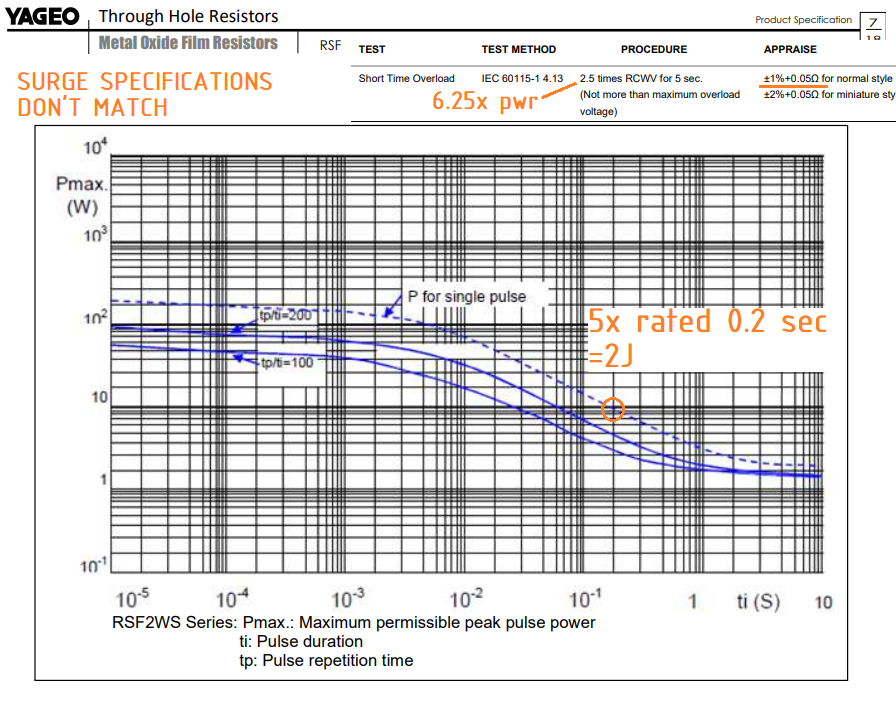
If we look at the Old Military
derating guide for pulse power in 3W resistors, we get 14 joules/rated
W at the 3W level. This power likely is conservative. A 2 or 3W wire
wound would work for 19 Joules.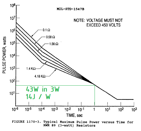
Below is the Raw data for the 2.5 second run from analog results plot above. It is taken at 138V line voltage with 0.22A on the output high voltage.
The secondary of the transformer sees 0.510A. I don't like running commercial transformers at their rated current because they get very hot. I like to use them at less than 70% of rated so that the copper loss is half of maximum ratings.
The primary current draw (high line, maximum load) was 2.7 amps. This is 372 VA input for 110W output. The input's "true" power is 142W for the 110W output.
vhv2_a: AVG(v(hv2))=510.246 FROM
0.330166 TO 0.380166
vhv1_a: AVG(v(hv1))=512.354 FROM 0.330166 TO 0.380166
r39_a: AVG(v(pwr_r39))=-0.00065924 FROM 0.330166 TO 0.380166
r20_a: AVG(v(pwr_r20))=0.00488848 FROM 0.330166 TO 0.380166
biasr_a: AVG(v(pwr_biasr))=0.348992 FROM 0.330166 TO 0.380166
biasr2_a: AVG(v(pwr_biasr2))=0.373181 FROM 0.330166 TO 0.380166
m1_a: AVG(v(pwr_m1))=0.000568521 FROM 0.330166 TO 0.380166
m4_a: AVG(v(pwr_m4))=0.386858 FROM 0.330166 TO 0.380166
m5_a: AVG(v(pwr_m5))=0.393883 FROM 0.330166 TO 0.380166
pout_a: MAX(v(pwr_out))=39.8294 FROM 0.330166 TO 0.380166
pin_a: MAX(v(pwr_in))=47.2236 FROM 0.330166 TO 0.380166
ploss_a: MAX(v(pwr_loss))=7.40974 FROM 0.330166 TO 0.380166
p_t1_a: MAX(v(pwr_t1))=4.03221 FROM 0.330166 TO 0.380166
irms_t1_a: MAX(v(i_rms_t1)**0.5)=0.218992 FROM 0.330166 TO 0.380166
irms_c7_a: MAX(v(i_rms_c7)**0.5)=0.205454 FROM 0.330166 TO 0.380166
p_ctrl_a: MAX(v(pwr_controller))=1.80279 FROM 0.330166 TO 0.380166
i_r6_a: AVG(i(r6))=0.00536809 FROM 0.330166 TO 0.380166
i_bq6_a: AVG(ib(q6))=0.00363409 FROM 0.330166 TO 0.380166
tvs_pk_a: MAX(v(pwr_tvs))=0.00856794 FROM 0.330166 TO 0.380166
sec_snub_a: MAX(v(pwr_sec_snub))=0.324626 FROM 0.330166 TO 0.380166
vhv2_b: AVG(v(hv2))=499.513 FROM
2.43017 TO 2.48017
vhv1_b: AVG(v(hv1))=506.144 FROM 2.43017 TO 2.48017
r39_b: AVG(v(pwr_r39))=-0.00182384 FROM 2.43017 TO 2.48017
r20_b: AVG(v(pwr_r20))=6.19045e-008 FROM 2.43017 TO 2.48017
biasr_b: AVG(v(pwr_biasr))=0.54188 FROM 2.43017 TO 2.48017
biasr2_b: AVG(v(pwr_biasr2))=0.543593 FROM 2.43017 TO 2.48017
m1_b: AVG(v(pwr_m1))=0.000446568 FROM 2.43017 TO 2.48017
m4_b: AVG(v(pwr_m4))=0.973054 FROM 2.43017 TO 2.48017
m5_b: AVG(v(pwr_m5))=0.980803 FROM 2.43017 TO 2.48017
pout_b: MAX(v(pwr_out))=114.101 FROM 2.43017 TO 2.48017
pin_b: MAX(v(pwr_in))=142.345 FROM 2.43017 TO 2.48017
ploss_b: MAX(v(pwr_loss))=28.3071 FROM 2.43017 TO 2.48017
p_t1_b: MAX(v(pwr_t1))=21.5025 FROM 2.43017 TO 2.48017
irms_t1_b: MAX(v(i_rms_t1)**0.5)=0.510581 FROM 2.43017 TO 2.48017
irms_c7_b: MAX(v(i_rms_c7)**0.5)=0.467561 FROM 2.43017 TO 2.48017
irms_input_b:
MAX(v(i_rms_input)**0.5)=2.7853 FROM 2.43016 TO 2.48016
p_ctrl_b: MAX(v(pwr_controller))=3.40798 FROM 2.43017 TO
2.48017*******
i_r6_b: AVG(i(r6))=0.00705922 FROM 2.43017 TO 2.48017
i_bq6_b: AVG(ib(q6))=0.0053591 FROM 2.43017 TO 2.48017
r20_joules: MAX(-v(r20_j))=19.2925 FROM 0 TO 2.501
tvs_pk: MAX(v(pwr_tvs))=7.23526 FROM 0 TO 2.501
tvs_pk_b: MAX(v(pwr_tvs))=0.0055314 FROM 2.43017 TO 2.48017
sec_snub: MAX(v(pwr_sec_snub))=0.504373 FROM 0 TO 2.501
sec_snub_b: MAX(v(pwr_sec_snub))=0.390495 FROM 2.43017 TO 2.48017
Do not try to build this on one of those plug-in "Experimenter Proto-Boards".
The voltages are too high for this board.
The circuit is too sensitive to parasitic resistances and capacitances to use on this board.
If a part wiggles at the wrong time, you'll have a smoking mess on your work bench.
You can't attach scope probes or meters to the parts pushed into these board for the probes will pull the parts leads out of the board.
Resist the temptation to use one of these experimenter boards. They are fine if you just want to make lights blink from a 9V battery circuit. They will not work in this application.
You could build this with point-to-point soldering on copper-free perfboard. The circuit will tolerate a socket for the IC, but be careful with M1's ESD sensitivity.
Watch the spacing between nodes at ground and nodes at 300V and 500V. Skip at least "1 row of holes" between the 300V parts and ground and "1 row of holes" between the input voltage and the output voltage. The "1 row" counts from the edge of a solder joint to the other edges of solder joints, not from the center of a lead to the center of a lead. Clean all the flux off the board before using it and then let the board dry before testing. Skip 2 rows for 500V differences.
1. Lay out a mixed leaded and surface mount ExpressPCB board for this design using 5mm creepage distances on the primary side (230V compatible) and IPC2221 uncoated spacing on the output side. 5mm is from 5mm UL creepage Group III is FR4 board material.
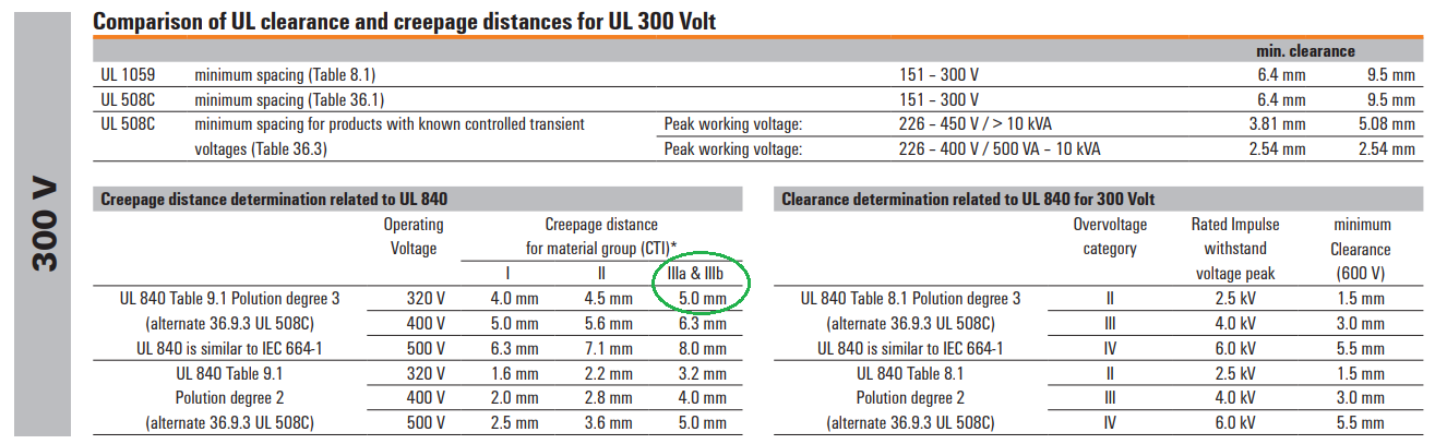
More on creepage from TI's TI Creepage Training
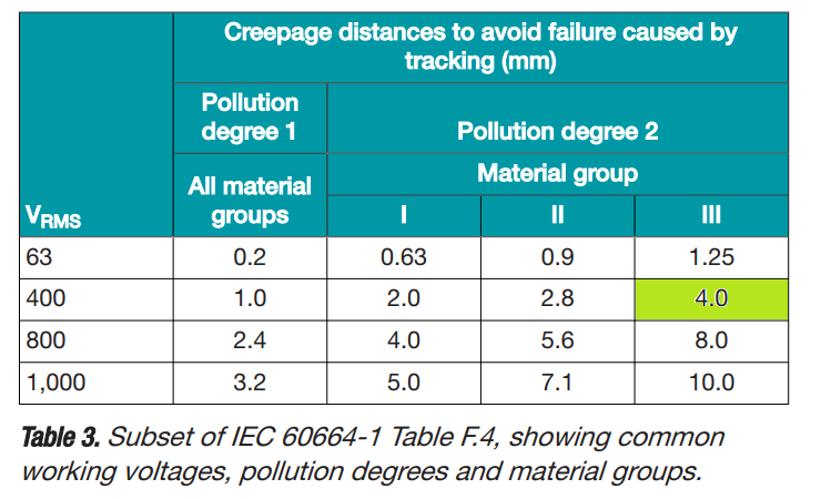
If we assume 360V peak for the 230V, no transients, IPC2221 calls out 98.4 mils creepage on a bare board which is 2.5mm.
DIY projects need a name. What should we call this beast?
This device stops the output voltage from rising when the peak output voltage on the first filter capacitor reaches a given value. The regulation is limited by the voltage ripple on the output capacitor. The switch is on the primary side.
Peak-Rip Regulator?
Rip-a-Peak Regulator?
P-R Regulator? (Ah... No.)
C-Peak Regulator?
PSCPeak Regulator? Primary Switched Capacitor Peak
regulator
PSPeakV Regulator? Primary Switched Peak Voltage Regulator
The "PSPeakV Regulator" for B+ Regulation (Pronounced Pesky Peak
Voltage regulator)
This design now goes back on the back burner so I can complete the documentation of a simpler circuit, but a circuit that needs a lot of justifications and warnings.
First version 20-May-2026, Last update 2-Jun-2026.
Changes to correct a couple font/ spelling issues do not count as an update.
.
 ( New 2024 index page.)
 _( Old
2003 index page.)
_( Old
2003 index page.)
 _(
AMP Second index page.)
( Fancy index page.)
_(
AMP Second index page.)
( Fancy index page.)