
SOLID STATE REPLACEMENT FOR A RECTIFIER
TUBE, SMALL VER 0
WITH DELAY AND SOFT START
DOES
NOT NEED TO USE FILAMENT WINDING FOR POWER
THE
SIZE TARGET IS THAT OF AN EZ80 TUBE
THE
PERFORMANCE TARGET IS TO BE CLOSE TO A 5AR4 TUBE
Oct 2025, Ver 0
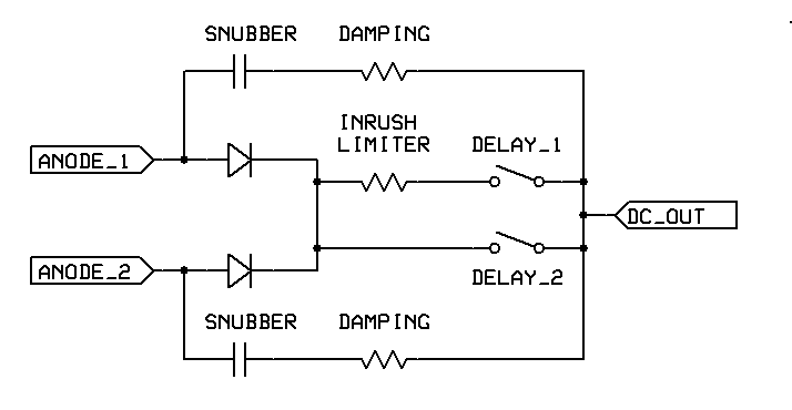
-
----------------------------------------------------------------------------------
-
Pros of a Solid State Rectifier:
As long as no aluminum electrolytics are used, solid state rectifiers will last for decades without replacement or change in performance.
It will have a lower forward voltage drop.
(This can be good or bad news.)
It can support larger capacitor banks
It can allow higher repetitive peak current draws (i.e., a larger first capacitor attaching to the rectifier.)
It can run cooler than a tube rectifier. Fewer watts lost inside a tuner or preamp is nice.
The turn-on delay can reset back to zero with a very short power off allowing for fast tube swapping.
It "MAY" be less expensive. A "larger
size" solid state rectifier often can cost less than a small one. This
design is for a small one.
Depending on the transformer, it may free up the diode's heater winding for other uses.
If replacing a tube rectifier with a solid state rectifier, the increase in B+ may allow for adding a voltage regulator or an active filter.
Pros of a Tube Rectifier
It is Simple.
It is nostalgic. It glows in the dark in a nice way.
It may generate voltage "SAG" at high currents that can be desirable in guitar amps.
It has a nonlinear soft-start/startup profile that can be nicer than a simple resistive soft start. This can be important when large intrastage coupling caps are used.
The Tube Ratings have a "Sense of Humour." If you briefly exceed the parts ratings, the tube rectifier often survives and just wears out faster. If you exceed ratings on a solid state rectifier, it will throw a "Hissy Snap Boom Fit" and the blue smoke will come out quickly giving us a dead rectifier. (i.e., don't push the ratings on solid state.)
The higher voltage drop of a tube
rectifier is often accounted for in a design. If switching to a solid
state rectifier, B+ may be higher, which may or may not be
desirable.This often is fixed with an external "Sand Cast" resistor
(not a film resistor) in the cathode to the first capacitor. This will
mimic the losses in the tube rectifier.
Referencing the vacuum tube rectifier table below, this design should attempt:
PiV >=1500Vpk (Part and PWB limited) [Result: 1600V. ]
Ipk >=750mA (Thermal / PWB size limited) [Result: Over 1 amp, use the LTSPICE Model to check. ]
Isurge >= 900mA (Gate Drive Voltage and Transient Thermal Capacity limited) [Result: Over 2 amps, use the LTSPICE Model to check. ]
Idcout >= 250mA (Thermal / PWB surface area limited. Besides the load current, this is impacted by the resistance of the transformer secondary and the size of the external capacitor the rectifier feeds.)
[Result: 250mA with approximately 40C board rise at 400V-0-400Vrms and 100uF/2 ohm ESR output capacitor.]
Vac >= 550-0-550V (Part and PWB limited) [Result: 565V-0-565Vrms FWCT surge. 447V-0-447Vrms steady state possible. Less than 400V-0-400V recommended.]
Max Cap >= 50uF (This often refers only to just the first cap after the diode. This design will be concerned with the total capacitance on B+ (the high voltage output), not just the first capacitor. Note that a large first capacitor after the rectifier (tube or solid state) increases the RMS current in the transformer and in the first capacitor.)
[Result: 100uF validated at 447V-0-447Vrms FWCT, >100uF at lower voltages.]
Dimension goals:
22.2 mm = 0.874 inches ( Goal for Width and Height (cap and 5W resistor size.) I'm OK with a square peg for a round hole.)
60.3 mm = 2.37 inches (Stretch goal for length. This was not met. We end up needing 2.5")
71.4 mm = 2.81 inches (Hard limit goal for length)
Data from a couple tube rectifiers:
| Diameter (mm) |
HT (mm) |
Filament Volts |
Filament Amps |
Max Cap UF |
PiV | Ipk mA Recurring |
Ipk Surge |
|
| EZ81 JJ | 22.2 | 71.4 | 6.3 | 1 | 50 | 1300 | 500 | |
| EZ80 | 22.2 | 60.3 | 6.3 | 0.6 | 50 | 1000 | 370 | |
| 6V4 | 22.2 | 66.7 | 6.3 | 0.6 | 50 | 980 | 270 | 900 |
| GZ34 | 33.3 | 72 | 5 | 1.9 | 60 | 1500 | 750 | |
| 5AR4/GZ34 | 38.1 | 72 | 5 | 1.9 | 60 | 1500 | 750 | |
| Max | 38.1 | 72 | 6.3 | 1.9 | 60 | 1500 | 750 | 900 |
| Vcath | Rint 100mA | IDC1 | Vac | Rt (2X) | ||||
| EZ81 JJ | 500 | 150 | 160 | 250 | 150 | |||
| EZ80 | 500 | 265 | 90 | 250 | 125 | |||
| 6V4 | 500 | TBD | 90 | 250 | 125 | |||
| GZ34 | N/A | 85 | 250 | 300 | 75 | |||
| 5AR4/GZ34 | N/A | 85 | 250 | 300 | 75 | |||
| Max | 500 | 265 | 250 | 300 | 150 | |||
| IDC2 | VDC2 | Rt2 (2X) | IDC3 | VDC3 | Rt3 ((2x) | Max AC | ||
| EZ81 JJ | 150 | 350 | 230 | 100 | 450 | 210 | ||
| EZ80 | 90 | 300 | 215 | 90 | 350 | 300 | ||
| 6V4 | 90 | 300 | 215 | 90 | 350 | 300 | ||
| GZ34 | 250 | 350 | 100 | 250 | 400 | 125 | 550-0-550 | |
| 5AR4/GZ34 | 250 | 350 | 100 | 250 | 400 | 125 | 550-0-550 | |
| Max | 250 | 350 | 230 | 250 | 450 | 300 |
PIV.
Peak Inverse Voltage. This is the absolute maximum reverse voltage we can apply from the output (Cathode) to the Anode. This value must be respected under all conditions, transients, no load, high line, etc.
The peak to peak end to end voltage from the unloaded transformer at the high 50/60 Hz line (132Vac) often dominates the stress put on the rectifier's PIV.
Un-snubbed or poorly damped secondaries can have up to 2:1 voltage overshoots when the main power switch closes. This means the 1000V peak on the secondary of the transformer rings up to 2000V peak.
Full Wave Bridge vs Full Wave Center tap.
The Full Wave Bridge uses 4 diodes. At no load the capacitor rises to the full end to end peak voltage of the transformer (i.e. twice the voltage from one end to the center tap.) With this design, the two diodes going to ground are external to this PBA.
The Full Wave Center Tap uses 2 diodes. At no load, the capacitor rises to half the peak end to end voltage of the transformer (i.e. one end to the center tap.)

Max Output Capacitance
This value is set by the stresses in the rectifier from:
1. The energy adsorbed charging the "joules" ( 0.5 C Vout^2 ) into the output capacitors plus the energy absorbed by the rectifier from pulling the "load" from ground to the final voltage. The load current matters because of the turn-on delay, the tube's cathodes will be HOT when the tube's votlages rise and current will be drawn by the tubes from the high voltage supply.
2. The peak current draw in normal operation charging the output capacitance. The effective DCR of the transformer and the ESR of the capacitor help keep this peak current to a reasonable value.
C. We want to have a soft start to precharge the output capacitors before we close the final switch.
D. I'd like a "blinky" light on the board that lets me know the circuit is doing something without needing a DVM to check the high voltage. To make it smaller, I can omit this. But 18 seconds is a long time to wait wanting to know if anything is happening. F.
I'd like a small solder hole on top to attach a solder eyelet or
a hook to. This will be used as a support mechanism. I'm going
to pick a typical value for this resistor, this being a DIY
project means you can second guess me and use a different value
for your project.
G.
I want an extra hole on Anode_1 and/or Anode_2 to wire over to a
circuit like the "Disharginator." The target size for a #20 solid is 0.0323" max diameter
(untinned.) or for a #22 stranded 9/34 it is 0.0315"
diameter nominal. with a goal of fitting a #20 stranded 19/32 at
a 0.040" diameter nominal. With a hole tolerance of 0.0004", a
0.046" hole should fit all three.
H. If two (two sets) of external diodes are added to
this design, the design is to work in a Full Wave Bridge
application. Lets be greedy and fit two more holes on Anode_1
and/or Anode_2 for wires to run to the diodes for this function.
I. I'd like it to be able to be used with Choke input designs.
-
-
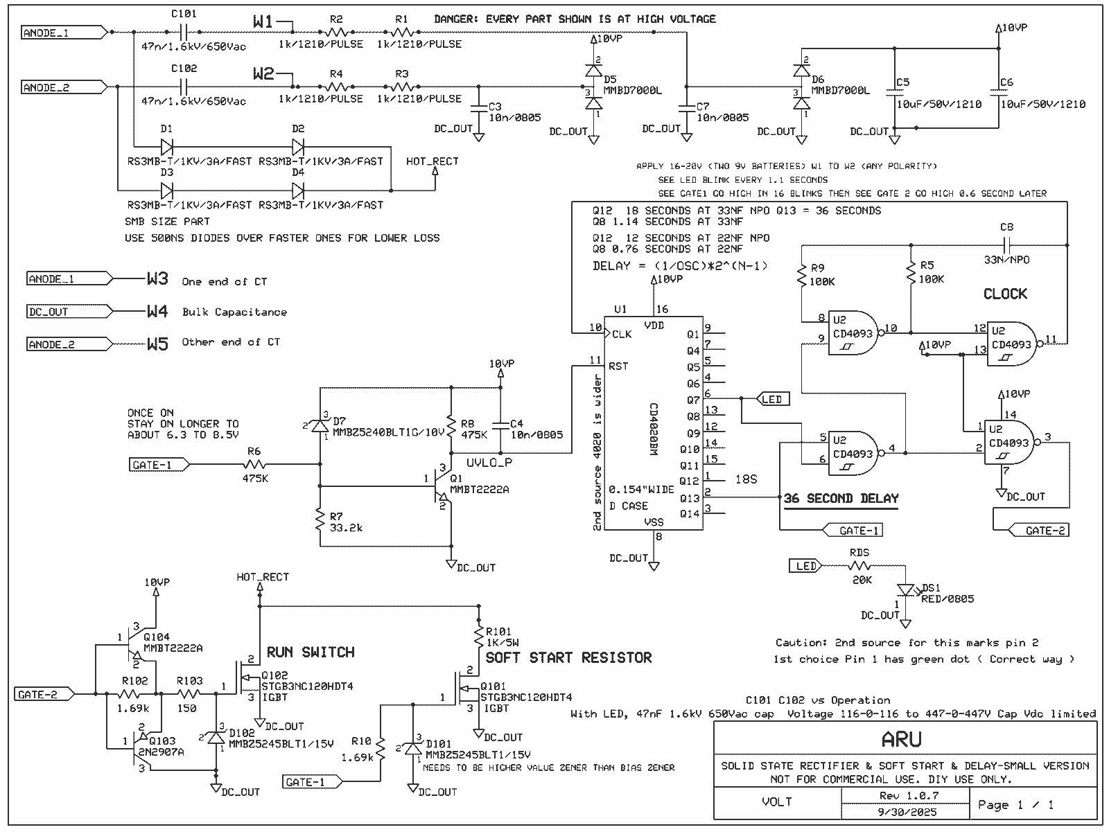
This is the 36 second delay version. The only change is that Gate-1 is now attached to U1-Q13. If you want 72 seconds of delay, move the trace going to Q13 to Q14.
A few cautions for those who are
designing one of these on your own. The high voltage
spacings have to be met under three different
conditions:
1. At initial power-up, the W1 and W2
sides of C1 and C2 will briefly pop up to the peak
unloaded high line voltage and then decay to "DC_OUT"
(0V). HOT_RECT after the diodes will be at the high
line unloaded voltage from the transformer. This
means there can be 1200V between these two nodes and
1200Vpk from these nodes to "DC_OUT" parts. How high
this voltage is allowed to be is mostly limited by the
MOSFET Voltage, the peak voltage rating of R1-R2 and
PWB trace spacing. During normal operation, the
voltage difference between these two nodes is less
than 3V, but we'll have to survive all of the voltage
stresses from the turn-on transient to get there.
2. When the soft start resistor is switched in, one side of the R101 resistor will be at DC_OUT and the other side (HOT_RECT) will be at the high line input voltage. DC_OUT starts at zero volts and now will begin slowly ramping up in voltage with respect to signal ground. Again the voltage from Q102 drain to the other control parts and copper is limited by the FET voltage ratings and a second set of PWB trace spacings.
3. In normal operation, there will be
DC_OUT between all the parts touching "DC_OUT" and the
chassis of the amplifier. There will be the Peak
transformer voltage from Anode 1 and Anode 2. There
will be the peak transformer voltage from Anode_1 or
Anode_2 to DC_OUT and to HOT_RECT. This voltage will
be limited by diode voltage ratings and a third set of
PWB Trace Spacings. However, HOT_RECT will be 3V or
less away from the parts on the DC_OUT "local ground
plane."
Surface mount parts are called out. Be gentle soldering the SMT ceramic capacitors, pre-warm the ceramic and never hit the part directly with the iron. Heat the land and flow the solder to the cap. Use a drop of water soluble flux on each part lead and each land before soldering.
If you are wanting higher performance, use a bigger PWB and switch D1-D4 to be SMC size diodes.and switch R1-R4 to be 6 pulse rated resistors instead of 4.
If you are wanting higher output voltages, put a circuit like this on the primary of the transformer, use a separate filament transformer and consider using a charge pump to make the high voltage DC output. Why a charge pump? The biggest reason is that the AC voltages are much lower. Corona and arcing is easily triggered by AC voltage and not as easily triggered as with DC voltages. The second reason is that there are many 240Vac output transformers out in the world that don't cost a lot. The price difference will pay for many diodes and capacitors.
-
There is no C1 and C2. They became C101 and C102 on the bottom of the card.
| Qty | Name | Order | Part ID |
| 3 | 10n/0805 | 478-10823-1-ND | C3,C4,C7 |
| 2 | 10uF/50V/1210 | 587-6160-1-ND | C5,C6 |
| 1 | 33N/NPO | 445-6950-1-ND | C8 |
| 2 | 47n/1.6kV/650Vac | R76TN24704040J | C101,C102 |
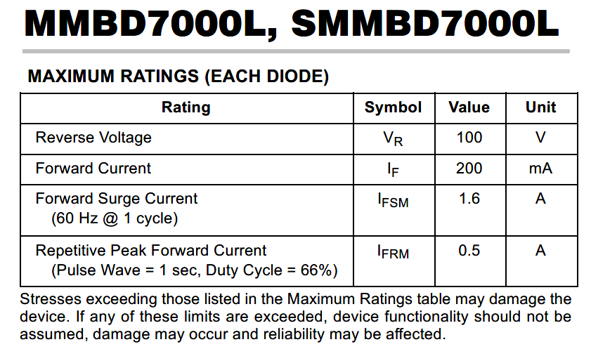
| 2 | MMBD7000L | MMBD7000LT1INCT-ND | D5,D6 |
| 1 | MMBZ5240BLT1G/10V | MMBZ5240BLT1GOSCT-ND | D7 |
| 2 | MMBZ5245BLT1/15V | MMBZ5245BLT1GOSCT-ND | D101,D102 |
| 1 | RED/0805 | 1497-XZCM2CRK54WA-1VFCT-ND | DS1 |
| 4 | RS3MB-T/1KV/3A/FAST | RS3MB-T | D1,D2,D3,D4 |
| 1 | 2N2907A | MMBT2907ALT1GOSCT-ND | Q103 |
| 2 | MMBT2222A | MMBT2222A-FDICT-ND | Q1,Q104 |
| 2 | STGB3NC120HDT4 | 497-11215-1-ND | Q101,Q102 |
| 2 | 1.69k | 541-1.69KCCT-ND | R10,R102 |
| 1 | 150 | 541-150CCT-ND | R103 |
| 2 | 100K | 541-100KCCT-ND | R5,R9 |
| 1 | 1K/5W | WS5M1001JCT-ND | R101 |
| 4 | 1k/1210/PULSE | CRCW12101K00FKEAHP | R1,R2,R3,R4 |
| 1 | 20K | 541-20.0KCCT-ND | RDS |
| 1 | 33.2k | 541-33.2KCCT-ND | R7 |
| 2 | 475K | 541-475KCCT-ND | R6,R8 |
| 1 | CD4020BM | NLV14020BDR2G-ND | U1 |
| 1 | CD4093 | 296-25956-1-ND | U2 |
| Alternate Parts | |||
| 1 | 1K/5W | 749-AC05000001001JAC00CT-ND | Z_ALT_R3 |
| 1 | 1K/5W | WS5M1001JCT-ND | Z_ALT_R3A |
| 1 | 22N/NPO | 445-6949-1-ND | Z_ALT_C4 |
| 1 | 33n/700Vac | 399-12622-ND | Z_ALT_C101-02 |
| 1 | 33n/700Vac | B32672L8103J000 | Z_ALT_C2OLD |
| 1 | 47n/700Vac/Tight Fit | PHE450SD5470JR06L2 | Z_ALT_C101-02A |
| 1 | 68n/1.6kV/650Vac | 399-R76TN26805050J-ND | Z_ALT_C101-02B |
| 1 | STH13N120K5-2AG | 497-STH13N120K5-2AGCT-ND | ZALT_Q102 |
| 1 | STH13N120K5-2AG | 497-STH13N120K5-2AGCT-ND | Z_ALT_Q101 |
Purchase your parts from a place that has quality control over their parts like Digikey, Mouser etc. I've heard complaints about parts coming from Ebay etc.
You will also want liquid flux (water soluble), an "acid brush", a pint of 70% Isopropyl Alcohol, a solvent dispenser and a bottle/can of conformal coating (self extinguishing).
I prefer to use "leaded" solder. It
will never grow tin
whiskers. I still
haven't seen proof
that lead free RoHS
solder is whisker free
when the time duration
is measured in decades
instead of 90 day
warranties. Conformal
coat will not stop tin
whisker growth, but it
does reduce the risk..
-
The section is on the Printed Wiring Board Layout and related notes. For analog/ power cards, I prefer most traces to be wider than 10 mils and I prefer 20 mil via diameters versus the smallest ones available. A 20 mil via has an aspect ratio of 3:1 on a 62 mil board. An aspect ratio of 3 is reasonably.strong. Vias in the PWB will need a wider trace (or teardrop) attaching to them where they connect to 15 mil or thinner traces.
The finished 2.5" by 3.8" EXPRESS PCB board surface is not full. This allows you to either make copies of this circuit on the board and/or add another circuit to the board, such as adding in the "Discharginator." The Discharginator Design
-

With
a 62 mil thick
board and 4
layers, we
"should" get
20 mils
between
layers. 20
mils at
100V/mil
through the
PWB will
support 2kV
peak. The
100V/mil is
what most
"aged" PWBs
are rated to
take. I would
not run this
anywhere near
a 100Vac/mil
stress, but a
100Vdc/mil is
feasible. AC
voltage
between layers
of a PWB can
excite corona
in any trapped
air bubbles in
the
fiberglass.
Air bubbles
can cause us
to have a bad
day later on
in the use of
the product.
Corona
is a "wear
out"
mechanism.
Having corona
usually (not
always) does
not lead to
immediate
failure.
So spend a lot
of effort on
AC voltage
stresses that
are always
present, spend
a bit less
effort on
steady state
DC voltage
stresses and
spend just a
reasonable
effort on
short term
transient high
voltage
stresses. Hey,
a reasonable
effort is not
blowing the
effort on a
couple of
parts. It is
using IPC
voltage
spacing
instead of the
OLD ENG RULE
spacing.
-
Layout Effort: Using temporary Keep-outs on the Silk Screen to assist in parts placement
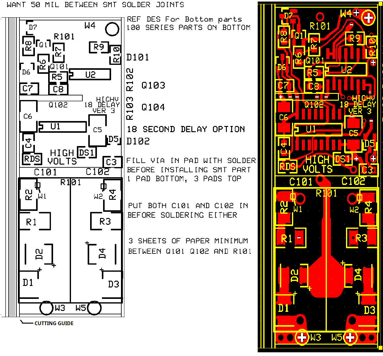
On the Silk Screen, I temporarily drew 60 mil radius 12 mil line thickness circles to generate "keep-outs" to enforce a 130 ml spacing between parts for 1200Vpk separation. The only place this didn't work was under the SMB 1000V diodes which had a 80 mil spacing land to land. SMC size diodes would offer a better spacing between the solder joints, but the parts would not fit in the desired X or Y dimensions.
Parts of the silk screen keep-out markings were to address Layer 1 issues, other keep-outs were to address the bottom layer issues. Between the two FETs, there is a small strip of vias that are 120 mil from Q101 and also 125 mil from Q102. These vias allowed the other parts to actually hook up successfully. These vias only see voltage stress during the inrush delay.
Before the final version of the board is ordered, most of these guide vias will be removed. Below is an early stage where I'm roughing in the power parts. Parts on the bottom start with a REF DES of 101 to help me easily identify what side of the card the part is on. In ExpressPCB Classic, we don't get to put silk screen on the back of the card and with high voltage present on parts, we can't afford to etch the REFDES into the bottom copper.
For ease of soldering, I'm trying to have 50 mils land to land on parts and on parts other than resistors and caps, I made the lands a bit longer on SO packages to help with hand soldering.
On the HV parts I built round knobs on the corners to lower the E-Field from the high voltage. The Diodes in this picture don't have the corona rounding knobs on the corners yet, they do in the final version.
-
-
-
-
Layout Effort: Top Layer Changes for the 36 Second Delay Version

-
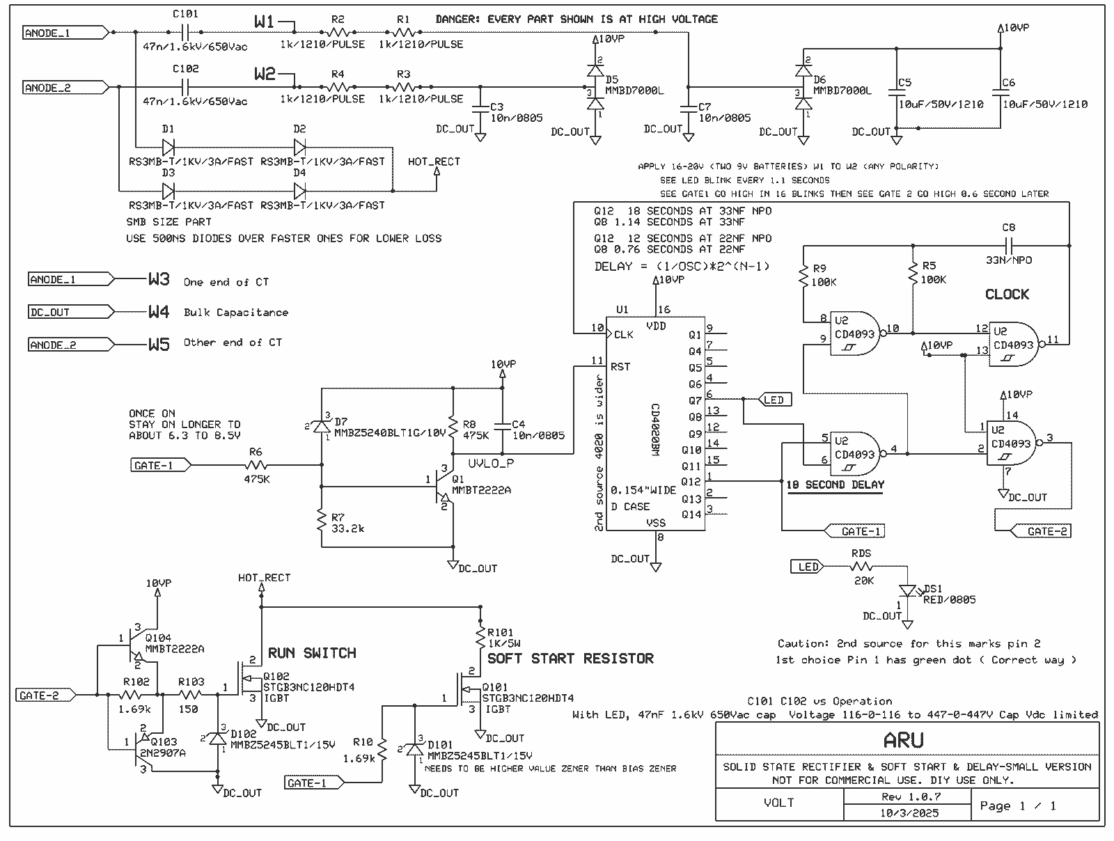
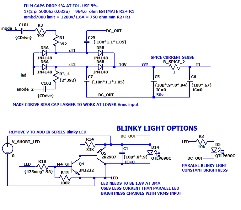
1. A charge pump connected to the anodes of the diodes provides power to the control circuit. The design requires both anodes to see an AC voltage to power the circuit. This "C_Bias" capacitor with a series resistor "R_bias" also functions as a snubber for Anode_1 and Anode_2.
2. When the internal circuit power (10V to DC_out) is low in voltage, we hold the timer (CD4020) in RESET. In this case UVLO_P high is in voltage to RESET the counter. When the 10V rail rises far enough in voltage, we pull UVLO_P low and allow the counter to run.
3. A two inverting logic gate RC oscillator (clock) runs whenever either of the output MOSFETs is off. We turn the clock off when both FETs are turned on to reduce the power needed by the control circuit.
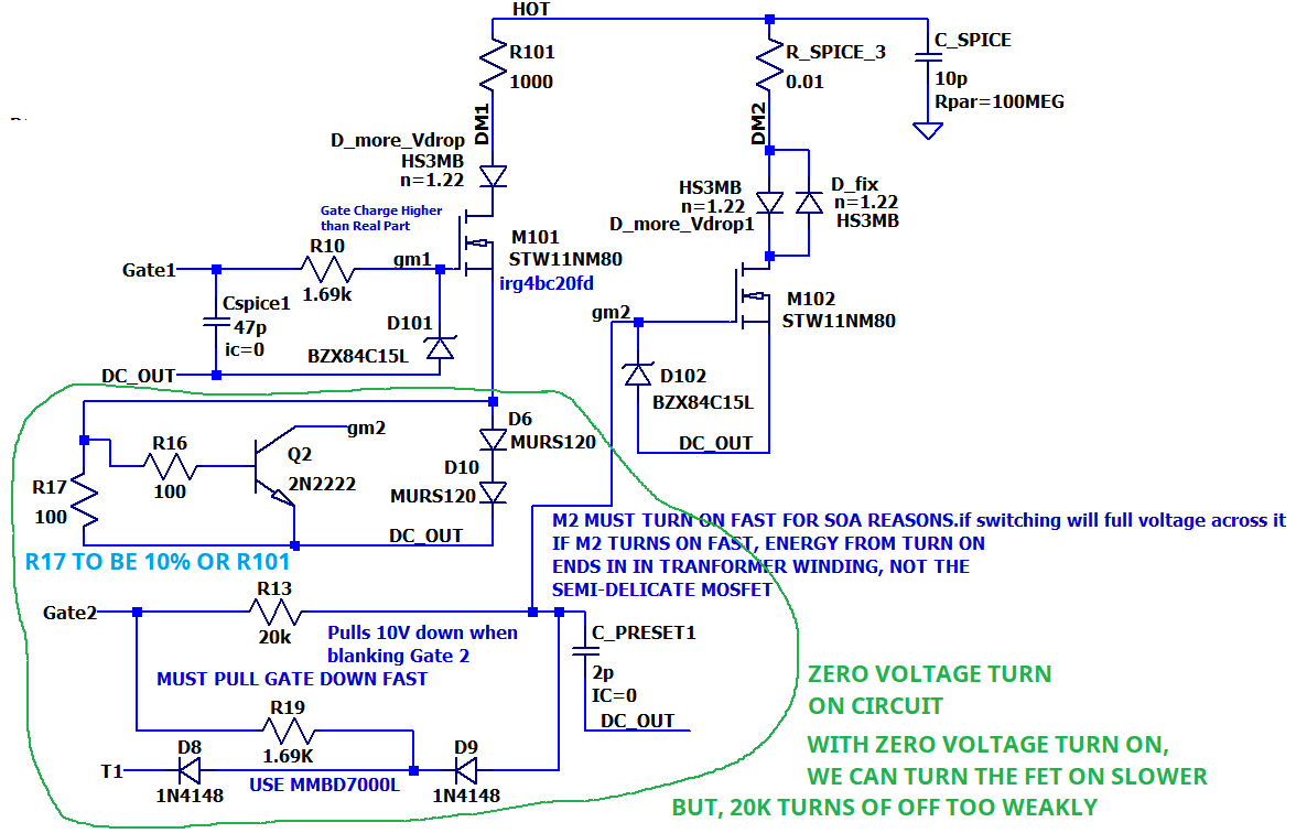
4. After an 18 second delay, we turn the soft-start MOSFET (GATE1) on to precharge the output caps through a wire wound resistor. A wire wound is used to take advantage of its high pulse voltage rating and its 5 to 10 times rated power for 5 second surge rating. Because the surge current in this first MOSFET is limited by a series resistor, we can turn this MOSFET (or IGBT) on moderately slowly (in several microseconds vs less than a microsecond.)
5. After 0.6 seconds of precharging the DC output with MOSFET 1, we turn the RUN MOSFET 2 (GATE2) on to fully enable the power diodes. Because the inrush current when GATE2 turns on is only limited by transformer parasitics, this FET must be turned on quickly to avoid a SOA overstress and we have to be concerned about the minimum resistance in the power transformer. This minimum resistance concern is no different than with a tube rectifier, but this solid state rectifier version can handle a larger inrush current than what the tube can.
6. An LED is included on the board for non-contact trouble shooting. It is not intended to run this LED off the PBA to the chassis of the equipment. If the LED was replaced with an optocoupler, the optocoupler could drive an external blinking light. When the output is in the delay mode, the LED blinks every 1.1 seconds. The LED will not be bright because of the transient stress limitations of the "R_Bias" parts.
-
With T1 (the 10V rail) at 11.66V max and 1.9V drop in a series LED, the circuit needs the current shown in the table below to run: We'll include current to drive the 475K resistor to drive a series LED blinking circuit, but not the current to power a parallel driven LED. I'm going to show the change in voltage (Q=C*V) driving the two 10nF EMI capacitors attached to the diode bridge as a power loss.
uA to run 11.66V 85C
Loss EMI caps
97.87 Clock (no Idd)
2.00 parts 83.70 4093 4 gates
50.00 Hz 365.00 4020
1.00E-08 cap 43.30 UVLO
I(R7) + I(R8) + Ibase
14.26 delta V 23.97 Blinking Resistor
1.10 Tol 0.00 Extra Current
613.84 sub total
1.10 Temp 17.25 loss to two EMI Caps
1.73E-05 Amps 631.10 UA needed
17.25 uA The HV film charge pump cap tolerance is +/- 10%, -2% temperature with a 4% loss for aging (0.84 factor). At 50 Hz, we would like to operate below 100V-0-100V and it looks like we can operate down to 94V per leg (94V-0-94V) with the LED removed and a 33nF cap.
Knowing Q = I * T = C * delta V, where T = 1/line Frequency
The needed delta V = I * T/C = dV from the transformer is as follows:
dV is reduced by the voltage swing needed at the MMBD7000L diodes to generate the "T1" voltage. I'm going to ignore the voltage drop in the damping resistors.
dV xfmr = 631uA * (1/50Hz) / (2 caps * 33nF * 0.84) + 14.96V receive side
dV xfmr at low line = 241.9V pp
The low line factor is 105Vac/115Vac = 0.913
242V Xfmr pp needed at 115V / low line factor = 265Vpp nominal/sqrt(2) / 2 windings = 93.7Vrms
Or in a simpler to read table format:
I needed 6.31E-04 Freq 50.00 C Charge Pump 3.30E-08 num caos 2 C_tol 0.84
DV lost at EMI caps 14.26 Needed dV 241.93 Vrms 171.07 Half V at low line 85.53
Low line factor 0.91 Nominal V 93.68
PASSING: Xfmr rms = 171V ( 93.7V-0-93.7V ) at nominal 115V input. (82V out per leg at low line)
This range means it will work with the smaller 100-0-100 Hammond transformer. If you want to work to an even lower transformer voltage, drop the voltage rating on the plastic bias caps and buy a higher capacitance part. To get to 45V-0-45V, the cap would need to increase from 33nF to be 75nF with the LEDs removed.
PASSING: When the run FET is turned on, we want the UVLO_P to be harder to trip to the high state. When GATE2 goes high, the UVLO trip threshold drops to be just under 10V because of the resistor from Gate2 to Q1. This gives us more margin on the operating current. First order, the needed bias current will drop by
631uA * (11.6 - about 10V)/11.6 = 87uA giving about 14% more margin.
PASSING: When the rectifier changes to the low impedance "RUN" state, we want the card even harder to turn off. When GATE2 goes high, the clock is stopped. This adds additional 97uA * (1-14%) of margin (170 uA total margin.)
-
Operational Review 2: Bias Circuit Change for an additional 0.5mA for a Parallel LED Drive
Lets rerun the previous calculation to add in an additional 0.5mA load to drive an LED.
The bad news is that the 33nF bias capacitor dropout voltage changes from 93.7V to 233.4V
To keep the dropout voltage near 93.7V, the bias cap needs to be 82nF for 97.2V dropout or 100nF for 80.7V dropout. The MKP1O131005F00KSC9 0.1uF will support 600Vrms but only with 1000Vdc. This 1000Vdc limits the transformer RMS voltage to be
1000Vpp/2/sqrt(2)/1.15 line/1.1 reg = 307V-0-307Vrms (614Vrms end.)
600Vrms/1.15 line/1.1 reg = 437V-0-437Vrms [ i.e. The design is limited by DC Voltage rating. ]
Just looking at the capacitor limitations, let's put all of these calculations in a table format to make it easier to see:
uA to run controller 11.66V 85C 10nF EMI Losses
97.87 Clock (no Idd)
2.00 parts
83.70 4093 Total 4 gates
50.00 Hz
365.00 4020
1.00E-08 cap
43.30 UVLO I(R7)
+ I(R8) + Ibase
14.26 delta V
23.97 Blinking Resistor
1.10 Tol
500.00 UA Extra Current
For LED
1113.84 sub total
1.10 Temp
17.25 UA loss to
Two EMI Caps
1.73E-05 Amps
1131.10 UA needed
17.25 uA
-
High line will be 132V/115V. The unloaded voltage rise is 10%. Low line is 105V/115V.
5.00%, Margin Best Overall Choice Alternate 47nF Cap
More Margin
Difficult fit
Higher $
Check Rbias risk at
higher Vrms MaxCap for lower Vrms
Nom Usage
Some risk in Rbias
Surge energy rating
At High LineAlternate 68nF
Reduced Vrms
Allowed at
High lineCap for reduced
stresses above
400Vrms/LegMax Vrms/Leg Nom
No Margin
Just Capacitor Stresses447.2 553.4 447.2 335.4 553.4 Max Vrms/Leg Nom
Lowered by Margin
Just Capacitor Stresses424.8 525.7 424.8 318.6 525.7 Min Vrms/Leg Nom
Raised by Margin122.3 122.3 86.3 86.3 171.7 Min Vrms/Leg Nom
No margin116.5 116.5 82.2 82.2 163.5 Bias Cap Used R76TN24704040J PHE450SD5470JR06L2 R76TN26805050J R586N268050T0M MKP1U023305F00KSSD Cap DC rating 1600 2000 1600 1200 2000 Cap AC rating 650 700 650 600 700 C_bias nom
(Charge pump)4.70E-08 4.70E-08 6.80E-08 6.80E-08 3.30E-08 C_bias nom in nF 47 47 68 68 33 C_tol (min) 0.84 0.84 0.84 0.84 0.84 Note on cap Multi source Single source,
0.5 mm too wideSingle vender
No margin in Rbias
At high line limitSingle vender
Better margin in Rbias at high lineMulti source Controller Limits
uA needed 1131.10 1131.10 1131.10 1131.10 1131.10 I needed 1.13E-03 1.13E-03 1.13E-03 1.13E-03 1.13E-03 Freq 50.00 50.00 50.00 50.00 50.00 num caps 2 2 2 2 2 Min Vrms Calc
DV lost at EMI caps 14.26 14.26 14.26 14.26 14.26 Needed dV 300.76 300.76 212.28 212.28 422.30 Vrms min needed 212.67 212.67 150.11 150.11 298.61 Half leg Vrms needed
At low line106.33 106.33 75.05 75.05 149.31 Margin for Low Line
Low line factor 0.91 0.91 0.91 0.91 0.91 Lowest Nominal Vrms/Leg (115V rating) 116.46 116.46 82.20 82.20 163.53 Allowed at High Line
Vrms_nom XFMR
1 leg Loaded
Cap DC Rating447.2 559.0 447.2 335.4 559.0 Vrms_nom XFMR
1 leg Loaded
Cap AC Rating513.8 553.4 513.8 474.3 553.4 Highest Nominal Vnom/Leg
Min of two ratings447.2 553.4 447.2 335.4 553.4 Irms resistor 60Hz
Series with cap x1.10.011 0.014 0.016 0.012 0.010 1Kohm ohm loss 0.122 0.186 0.254 0.143 0.092 Turn-on Energy in
C_Bias at +10%0.015 0.023 0.022 0.012 0.016 Est DC out with Vmin applied @.85 FWCT 140 140 100 100 200 Est DC out with Vmax applied @.85 FWCT 510 630 510 380 630
The CD4020 allows slow rise times on its RESET pin, so we can filter it for noise with a small capacitor. Slow input rise times cause most 5V logic ICs to randomly break into oscillation and/or have high cross conduction currents with the internal transistors that are on the input pin and thus end up internally over heating (Note 1). Unfortunately, this issue isn't listed on the individual data sheets, but it is referenced in some of the application guides. Normally when you have a slow input rise time, you need to be using a "SCHMIDT" input gate to prevent problems.
(1) The "Boss" at work doesn't care if the circuit was shown with slow rise times on the input in an application note or a college textbook, what he's upset about is that there are field and factory problems. Beware of slow rise times on most logic devices. I really hate it when the first one built works and the 21st one doesn't.
Note: In the SPICE schematic, the REF DES can be different than the REF DES on the PBA.
C5 and C6 (shown below) are 10uF energy storage capacitors that keep the circuit alive during small dips in the input voltage. When the soft-start FET and/or run FET turn-on, the output voltage from the HV secondary can dip from the high surge current drawn. Without C5 and C6, the rail voltage T1 can dip in voltage and cause UVLO_P to go high, which will restart the 18 second timer. We also want protection against line voltage dips that are caused by dips in the 115V lines. The "Hold up" or "Ride Through" time provided by C5 and C6 is extended during a "Brown-out" because C_bias is still providing current, just not enough for continuous operation.
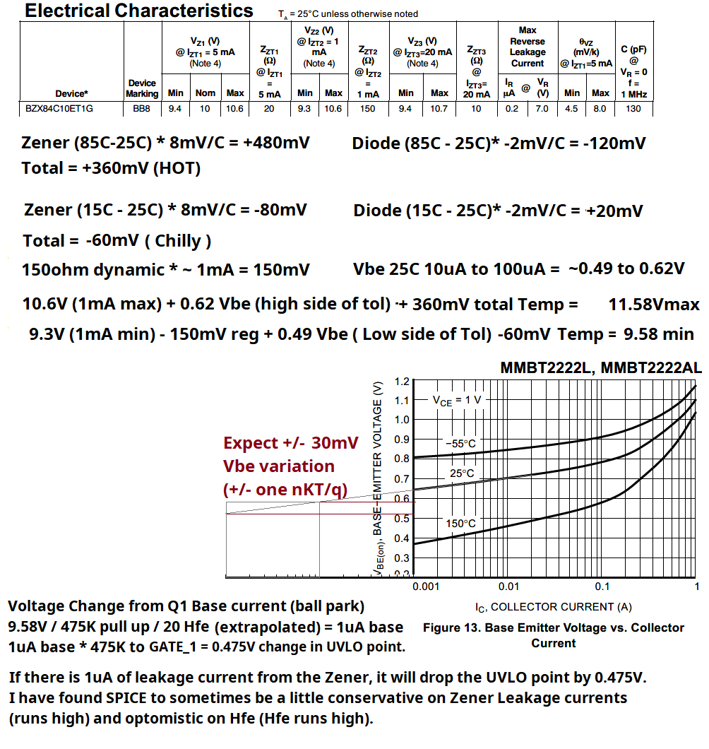
D7 zener and the base-emitter of Q1 set the control circuit's turn-on voltage and regulate the 10V rail. The lower we make this voltage, the easier it is to power this circuit, but the harder it is to get "R6", the hysteresis resistor, to work correctly. The voltage across D7 zener +0.8V needs to be at least 10% lower than the protection zeners that will be on the MOSFET gates. In this design these gate protection zeners are 15V so we are in good shape with either a 10V or 12V zener. With D7 at 12V, I had trouble getting the circuit to work with a 100V-0-100V transformer with the 115V at low line. With a 10V zener, I had some design margin. So I will be using a 10V zener for D7.
DO NOT APPLY A LAB POWER SUPPLY or BATTERY DIRECTLY TO 10V AND DC_OUT!
Q1 needs to be located on a cool area of the PWB, so keep it away from the "RUN MOSFET" and the input diodes. It is OK for it to be by the Soft-start FET. If the Soft-Start FET is running hot, something is broken.
R6/R7 force the circuit to run to a lower voltage on T1 once the GATE1 MOSFET is turned on. We want to avoid situations where we are stuck in repeated soft-start cycles (the soft start resistor will get hot enough to smell bad) and we don't want the RUN MOSFET to turn off immediately when the power is turned off to allow for the inductors in a choke input design to discharge to zero current before the RUN FET (Gate2) switches off.
C4 (10nF) is located by the CD4020 and filters out ripple on UVLO_P from ripple voltage on T1 when T1 is near the turn-on or turn off voltage for UVLO_P.
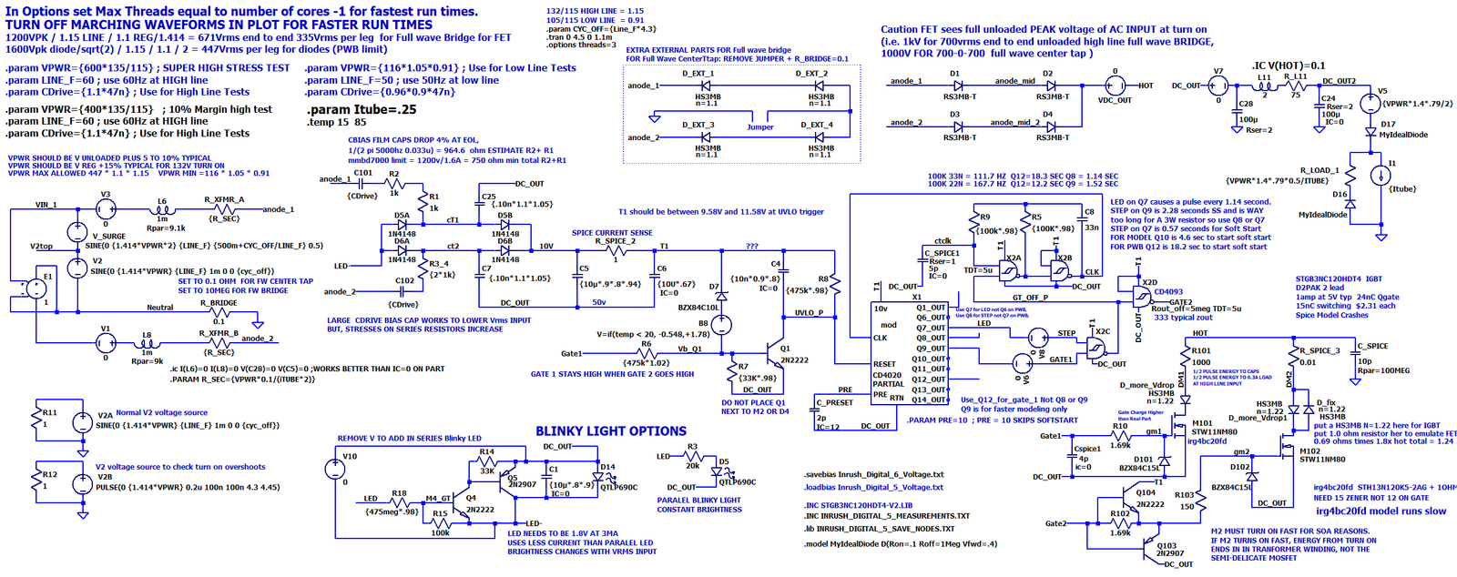
C_Preset and C_SPICE1 in the LTSPICE Schematic are SPICE tricks to let me control the initial conditions of the CD4020.at start up.
The CD4020 is my own model I developed at home and I've shared it with a few people. If you see a way to make it work better, email me.
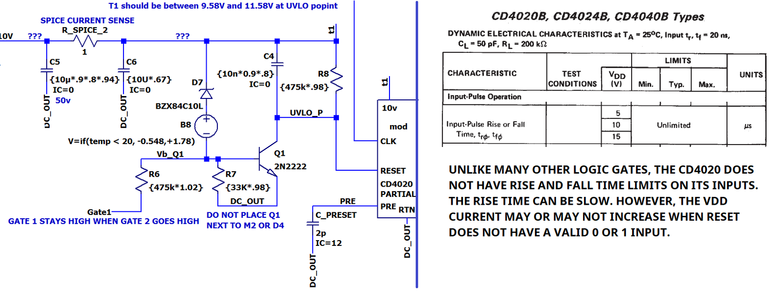

| Zener | Zener temp co | dT | Vbe | Vbe temp co | Z zener | I Z | Trip Voltage |
| 9.3 | 0.008 | -10 | 0.49 | -2.0E-03 | 150 | 1.00E-03 | 9.580 |
| 9.3 | 0.008 | -10 | 0.62 | -2.0E-03 | 150 | 1.00E-03 | 9.710 |
| 10.6 | 0.008 | 60 | 0.49 | -2.0E-03 | 150 | 0.00E+00 | 11.450 |
| 10.6 | 0.008 | 60 | 0.62 | -2.0E-03 | 150 | 0.00E+00 | 11.580 |
| Resistor Selection for UVLO_P MAX High Going | |||||
| Ibase Driving Rtop |
Rtop Nominal |
V from I_base |
R Ratio Needed |
R Tol | Min Vbe Resistor |
| 1.00E-06 | 475000 | 0.475 | 17.582 | 1.02 | 25968 |
| 1.00E-06 | 475000 | 0.475 | 13.895 | 1.02 | 32857 |
| 1.00E-06 | 475000 | 0.475 | 21.398 | 1.02 | 21336 |
| 1.00E-06 | 475000 | 0.475 | 16.911 | 1.02 | 26997 |
| 6.72E-08 | 475000 | 0.032 | 17.582 | 1.02 | 25968 |
| 6.81E-08 | 475000 | 0.032 | 13.895 | 1.02 | 32857 |
| 8.04E-08 | 475000 | 0.038 | 21.398 | 1.02 | 21336 |
| 8.13E-08 | 475000 | 0.039 | 16.911 | 1.02 | 26997 |
-
Picking 33.2 K for the base resistor, we get that UVLO_P should go high at 7.3 to 9.3V ignoring Zener leakage currents. The capacitor on UVLO_P will cause the voltage to rise slowly, so the 10V rail may be lower than this trip voltage when the RESET actually occurs.
| Analysis for UVLO_P Max High Going (no zener leakage) | ||||||
| Ibase Driving Rtop |
Vbe | Rtop | Rbase Total | Zener Trip Voltage |
UVLO_P High Voltage | Delta V |
| 1.00E-06 | 0.49 | 475000 | 33200 | 9.580 | 7.769 | 1.811 |
| 1.00E-06 | 0.62 | 475000 | 33200 | 9.710 | 9.704 | 0.006 |
| 1.00E-06 | 0.49 | 475000 | 33200 | 11.450 | 7.769 | 3.681 |
| 1.00E-06 | 0.62 | 475000 | 33200 | 11.580 | 9.704 | 1.876 |
| 0.00E+00 | 0.49 | 475000 | 33200 | 9.580 | 7.326 | 2.254 |
| 0.00E+00 | 0.62 | 475000 | 33200 | 9.710 | 9.261 | 0.449 |
| 0.00E+00 | 0.49 | 475000 | 33200 | 11.450 | 7.332 | 4.118 |
| 0.00E+00 | 0.62 | 475000 | 33200 | 11.580 | 9.267 | 2.313 |
-
The WS5 wire wound resistor (5 watt) used for the inrush resistor is rated for a surge power of 5X rated power times 10 seconds or 250 Joules at 25C (250 Joules at 25C). Unfortunately, several of the second sources for this part are only rated for 5X power for 5 seconds (125J at 25C). There are a couple of suppliers that only rate recurring surges and their rating is 10X lower than both of these parts.
With the 10X and 5X resistor supplier, the wire wound resistor's internal hot spot reaches 275C during the surge. To adjust the rated surge joules for 55C ambient during inrush, we linearly scale the allowed surge energy to 55C. We won't add in the 30C steady state rise to get to 85C for this calculation because the resistor is OFF before the surge current event. For long life, we should give this surge as much margin as we can, so running right up to the spec limit in normal operation is not a good idea.
250J * ( 275C - 55C ) /( 275C - 25C ) = 220J allowed for a part that is 5X rated for 10 seconds
125J * ( 275C - 55C ) /( 275C - 25C ) = 110J allowed for a part that is 5X rated for 5 seconds
The typical energy dumped into this resistor is
Joules = Capacitive energy transferred + Joules_Load
Joules load = Inrush Duration (T_inrush) * Power lost in inrush resistor to support the DC load
Joules = 0.5 Cout * Vout_inrush^2 + T_inrush * [ Vout_loaded - Vinrush ]^2 / Rinrush
Rload = Vout_loaded / Iload_Max
Rinrush = Inrush Resistor value + effective DCR of transformer secondary (Secondary DCR + reflected primary DCR)
This next design choice was rejected because
it required us to use two 5W resistors instead
of one. It was kept in the dialog for learning
reasons:
For a 1.25 second (max) T_inrush (1.17 sec nominal * 1.02 Rtol * 1.05 Ctol) into a "resistive" load at 447Vrms nominal, 10% load reg, 15% line reg, giving 673V loaded per the LTSPICE run
Vout_loaded = 673V (high line),
I load = 0.3A,
C load total = 200uF +10%/-20% = 220uF max
we get
Rload = 673/0.3 = 2240 ohm
Rinrush = 1K (Choice. Assume near zero DCR in transformer)
Vout_inrush = 673V * 2240 / (1000+2240) = 465V
Joules Cap = 0.5 * 200uF * (1+10%) * 465^2 = 23.8 Joules
Joules Load = 1.25 sec * (673-465)^2/1000 ohm =54.1 Joules
Total = 23.8+ 54.1 = 77.9 J
Re-running this with the load being a 0.3A current source
Vdrop in 1000 ohm inrush = 1K * 0.3A = 300V (approximate)
Vinrush = 673-300 = 373V estimate
Joules cap = 14.5
Joules load = 1.24 * 300^2 / 1000 = 112J
Total = 126 Joules.
126J is too much for the 5X 5 second 5W resistor. BUT!!! If we cut the inrush duration in half, the Joules Load drops in half and the 5X for 5 second source resistor works.
Let's look at a 0.625 second soft start duration with a 0.3A current source load. (Yes, current source loads exist.)
Joules cap = 0.5 * 200uF * 1.1 tol * 363V^2 = 14.5J
Joules load = 0.625 second * [673V-373V]^2/1000 = 56.3J
Total = 70.7 Joules (64% of the allowed 5X power for 5 seconds on a 5W resistor at 55C)
This indicates inrush soft start will be robust if the duration is 0.625 seconds and the resistor is a 1K 5W wirewound. Don't use a cheaper film resistor for this part.
0.625 seconds /3 = 208msec time constant.
1/(2 pi 208msec) = 0.76 Hz equivalent frequency of an RC circuit in a bias network.
208msec = 100K and 2.08uF or = 1K and 208uF or = 820 ohm and 254uF.
You could use a higher capacitive load on the output to slow the rise time of the high voltage. If we allow 2 time constants instead of 3. Roughly, a 2 RC time constant would allow 0.625/2 / 1.1 tol / 1Kohm = 0.284/Rinrush = 284uF total (it's not a lot bigger than 200uF.)
Advice for if you want to use a larger C_load at lower DC output voltages,
The inrush limiting resistor should be high enough in ohms to not pop the line fuse in the 0.625 seconds soft start period. The resistor value likely will still be a value close to Vout nominal / (2.2*I_load). The inrush resistor should also be small enough in ohms that the output voltage has stopped rising in 0.625 seconds (R * C_load < 0.625 seconds, preferably R * C_load between 0.284 seconds to 0.416 seconds).
Example Part 1/2: 330V out / (2.2 * 0.3A) = 500 ohms. If the unit is fused for 0.3A output max, this value should be good to use.
The smallest fuse on the 115V would be near (330V * 0.3A + 11W filament power )/115V / 0.8 margin = 0.76A ( I'd round up to 1.0A on the 115V side to start ).
Then keep the RC time constant of the inrush resistor and C_Load less than about 0.284.
Example Part 2.2: 0.284 / 500 ohm= 568uF max capacitance on Vout.
In this case, I'd use two 270uF caps (540uF total). One on the cathode of the rectifier and one after a series resistor or series inductor. There is an argument to rate them for 450V or even 500V so the caps don't vent if power is applied with the tubes pulled. (330V loaded / 0.85 shade) * 1.15 high line = 446V possible. The 1.1 unloaded factor isn't used because Shade works off the unloaded output voltage and then adds in the DCR / C_Load interaction in the 0.85 factor. Remember, the Shade multiplier factor can be higher or lower than 0.85.
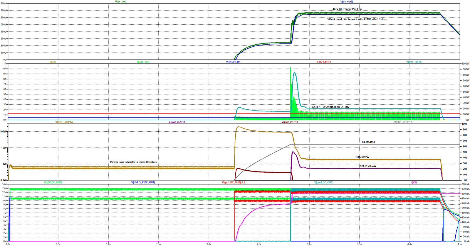
Here's the LTSPICE development model. The CD4020 and CD4093 are custom part models I made. The internal leakage on these two parts is set to the maximum leakage current at 85C. It does not change with temperature. This is with the 0.5mA LED drive (R3=20K)
-
Below is a 25C short duration run with the turn-on delay shortened (Gate1 attached to Q9 instead of Q12) to make the plots look better. This run is with a 47nF +10% capacitor for Cbias, 0.3A load and a nominal 447Vrms per leg (not the 400V in the picture above) input voltage run at high line. The DCR of the transformer secondary in the model is 43.7 ohms and there is a 200uF total capacitive load. This run is with the 0.5mA LED drive (20K resistor to LED). The hold up time gets approximately 45% longer with the 0.5mA LED drive vs the 1mA drive.
In the bottom window we can see the RED tracing (Gate1) going high 1/2 second before the Blue-GRN Gate2 trace. The output current is rising during this time (Violet trace.)
In the second from the bottom trace, the grayish trace, is the Inrush Joules and it runs at 65 Joules.
In the second from the top plot, the green trace, is the instantaneous current into the output caps.
For 250mA dc out, each leg of the
secondary
saw 0.363
Arms with 5%
regulation in
the
transformer.
The RMS
current from
the
transformer
will drop if
the
transformer's
regulation
changes from
5% to 10%.
Make sure the
power
transformer
used can
handle the RMS
current we are
putting in
each leg of
the
secondaries.
Free Convection Heat Flow
Calculator says for a 35C rise, we are
allowed 1.35W on the PWB. The 1.738W of loss at
250mA load will take the board from 40C to 85C,
a 45C rise. This is higher than I'd like to see.
The 150C HS3MB rectifying diodes will be running
hotter than the other parts, that reduces the
risk a little bit because it is a diode, but we
should try to improve on this.
| Watts
Loss at 250mA (85C) 447V / leg With 5% XFMR Reg |
% of Total | |
| 0.726 | 4 HS3MB Diodes Rated for 150C |
42.44% |
| 0.414 | M2 | 24.22% |
| 0.407 | Rbias Damping Resistors | 23.79% |
| 0.112 | Control Circuit | 6.55% |
| 0.050 | 4 Bias Diodes | 2.92% |
| 0.001 | Sense resistor | 0.08% |
| 0.000 | M1 | 0.01% |
| 1.711 | Total | |
-
| Watts
Loss at 250mA (85C) 400V / Leg 10% Transformer Regulation |
% of Total | % of 447V run | |
| 0.620 | 4 RS3MB Diodes Rated for 150C |
36.22% | -14.66% |
| 0.386 | M2 | 22.57% | -6.81% |
| 0.320 | Rbias Damping Resistors | 18.69% | -21.43% |
| 0.097 | Control Circuit | 5.67% | -13.44% |
| 0.013 | 4 Bias Diodes | 0.74% | -74.52% |
| 0.001 | Sense resistor | 0.08% | 0.00% |
| 0.000 | M1 | 0.01% | 17.13% |
| 1.437 | Total | ||
| 0.057 | Not on board in FWB diode Leakage Loss |
559V DC output at 0.25A | |
Free Convection Heat Flow Calculator predicts a rise from 47C to 85C at 1.459W. This is with free convection on both sides of PWB. To implement this, I doubled the width of the PWB, but kept the 2.5" Height the same. We may actually get some head conducted out the leads of the part. I've seen that happen more than once, but I don't know how to model it. What I can do is to increase the amount of copper trace area that is attaching to D2 and D4.
-

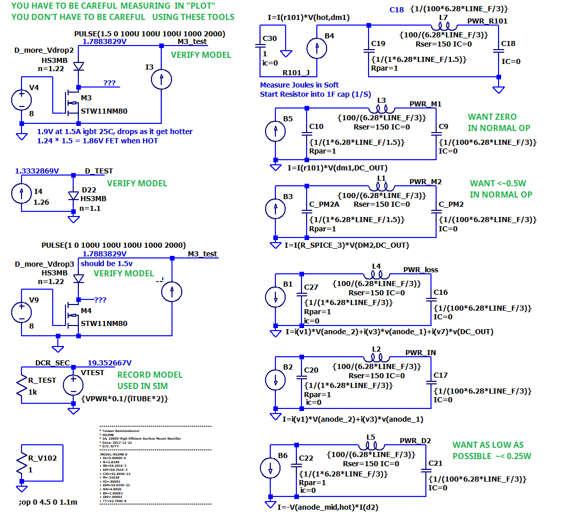
-
These are the measurement tools used in the LTSPICE model. You can fool yourself making measurements using the "measurement" function in "plot." RMS currents are hard to get exact. Integrals for energy can have errors in them if you are not careful. Using tools like this takes the worry out and makes the measurements capable of being made with a .MEAS command.
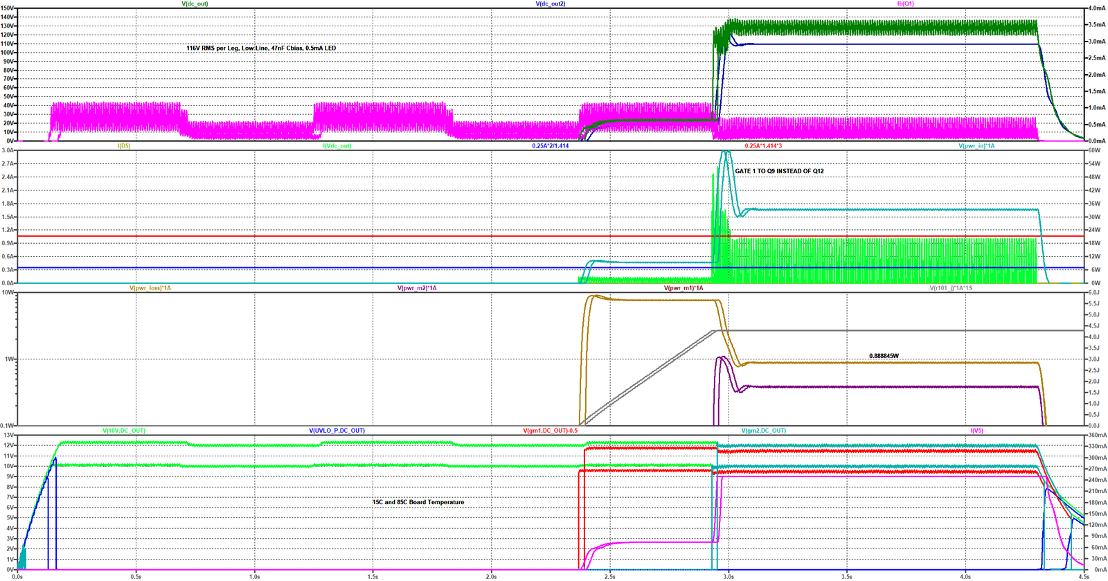
Below is the performance at 15C and 85C at 250mA 47nF at 116Vrms 50 Hz, 0.5mA LED load. The CD40xx models are already internally set to the max 85C bias current draw. The 10V zener voltage is corrected based on temperature to make it match the worst case trigger points for UVLO_P.
In the Top Plot, the purple run shows the base current of Q1 just barely over zero amps. This says we have a little margin at 116Vrms output with the 115V at low line input.
The output voltage is on the low side during the soft start period. It may be worthwhile to optimize the 5W resistor to a lower value, possibly 500 ohms with 116Vrms input (per leg).
All of the waveshapes are good. The top purple trace ( Ib(Q1) ) isn't hitting zero amps likely because of the margin I kept to drive one more 475K ohm resistor.
The 10V regulation at 15C was set to 10.3V and UVLO kicked at 8.48V. This gave a 25msec hold up duration at 15C (1mA LED). We have just over one cycle at 60Hz from complete loss of power before restarting the inrush limiter's 18 second timer. The actual 15C hold up time will be longer because U1 and U2's bias currents will have dropped and my model doesn't account for that. With the settings for 85C, the hold up is 110msec. Normal operation will be closer to half way in between.
For brown outs, the hold up time will increase because we'll still be getting some current from the "Bias Capacitors." A LTSPICE run with a drop from 116Vrms to 58Vrms increased the hold up time from 25msec to 95msec when using the 1mA LED.
If needed, the easiest thing we can do to improve this is to reduce the LED current from 1mA to 1/2 mA. We could change the 10uF capacitors to be 22uF, but the 22uF X7R are sole source and they make me nervous about the soldering risks (cracks). Dropping the LED current has an added benefit in that we can use a smaller Cbias capacitor (meaning drop the 68nF down to 47nF). This will help with the power loss in the damping resistors.
Each secondary winding was 389.41mA rms for the 300mAdc output. Each secondary only conducts 1/2 the time. The RMS in the FET was 549.85mArms and it conducts 100% of the time. ( A 1.4:1 ratio. ) The 50% conduction time causes a sqrt(1/2) ratio to occur between the RMS in one winding and the RMS through the FET and also through the transformer's primary.
From the green trace above, when Gate2 turns on, the RMS per secondary pushes up to 836.08mArms for 220msec before settling down. This is the current we have to worry about popping the fuse with.
-
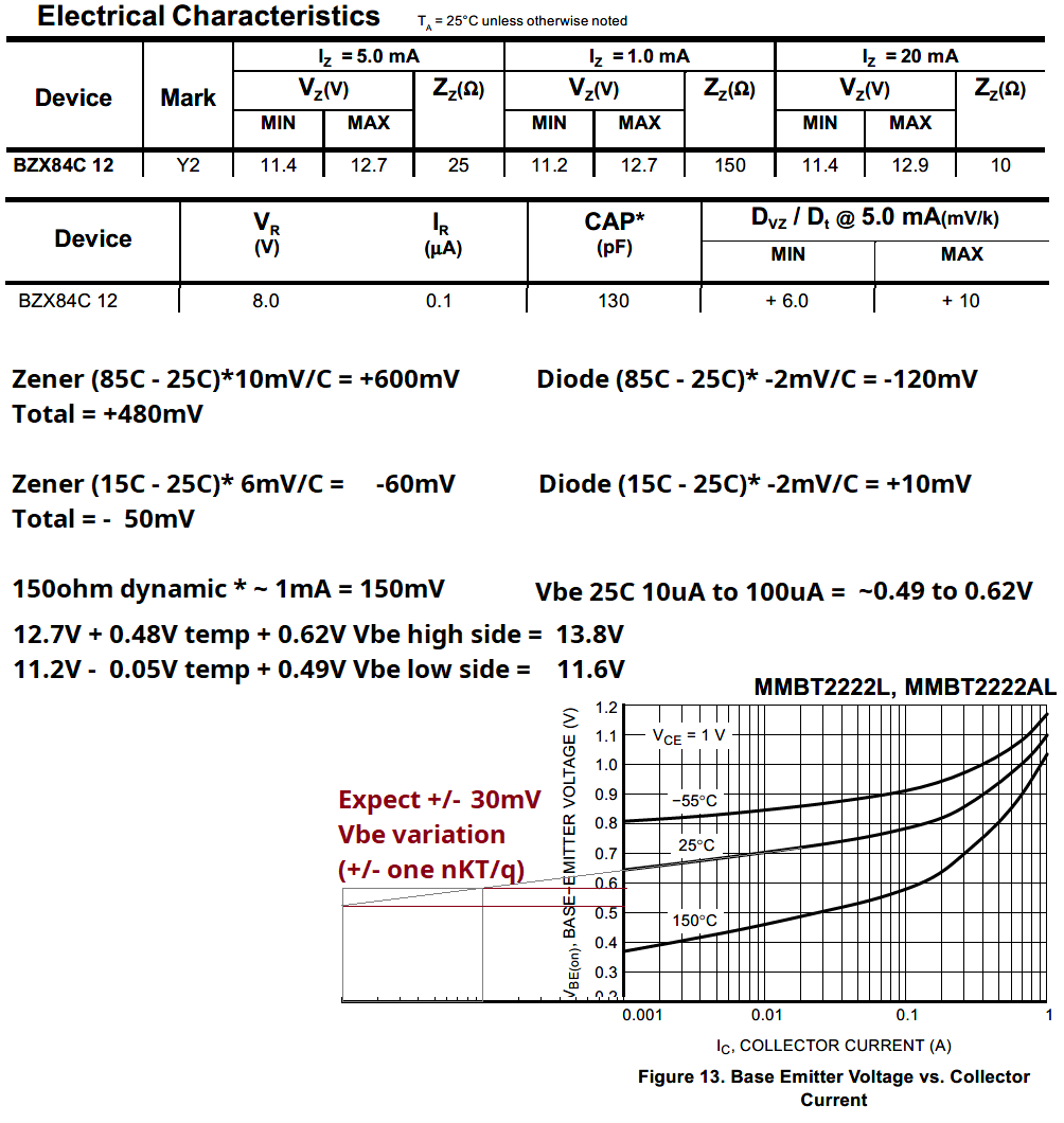
Per the SPICE Model, the gates are turning on at 12.5V (12V zener + 0.5V for a Vbe junction at low current). They will be turning off near 10V. If we do the calculations at 12.7V + tolerances, we have margin for lower voltages on the T1 bias voltage. In a different section of this file, the numbers for a 10V zener are calculated.
12V Zener +5% tolerance + Vbe of Diode + temperature effects need to be considered. This gives a Vdd operating voltage between 11.6 and 13.8V
From Philips, "Family Specifications, File under Integrated Circuits, IC04" we get a deep dive into the output resistance of the CD4093 series of parts. As Vdd gets higher, the part can drive more current. For an easier design effort, we'll do all the calculations at 10V instead of 15. We'll use the 25C curves for the part and scale the 25C performance by the ratio of the 85C to 25C performance.


-
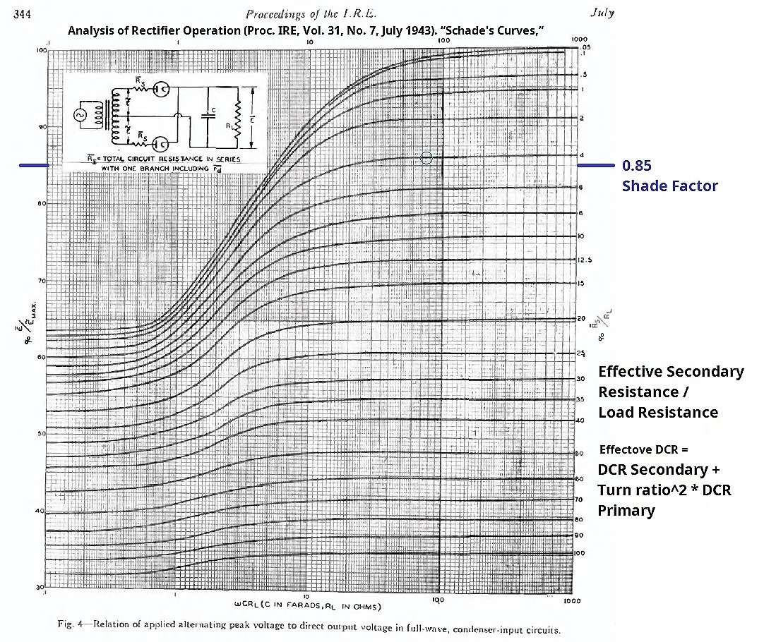
In the "Bias Circuit Change for an Additional Current for an LED Drive" table above I included a range of output voltages to expect with a 0.85 O.H. Shade factor. This means the rectified DC output voltage is 85% of the peak applied voltage. I've seen this factor go below 70%, but 85% is achievable and 90% can happen.
Shade's Output Voltage, A Quick Example:
100 ohm DCR secondary + 60 ohms reflected by primary = 160 ohm total series R (ignoring diode drops)
400V out/ 0.1A = 4000 ohm Rload
r/Rl = 160/4000 = 4%
w = 377 or (2 pi 60 Hz)
C = 50uF
wCRl = 75
Shade Factor = 0.87 from the chart for 332Vrms * sqrt(2) * 0.87 = 408V out
Duncan Amps PSUDII gave a factor of 0.85.1 for 400V out and PSUDII included the voltage drop from the diodes. The two calculation methods are close enough to matching!
As wCRl gets higher, the current stresses on the diodes, transformer and output capacitor go up. It's all a trade off. I've run into design issues with high wCRl causing the RMS current in the output cap and transformer secondary to exceed the rating for the part. With a low DCR secondary transformer, it's also pretty easy to exceed the diode's peak current rating too.
 Duncan Amps PSUD2 gives these results You run for 50msec after the delay because this in an integer number of 60 Hz cycles. With a FWCT shown below, the Duncan amps transformer voltage and DCR are for the "half winding." The transformer used below is a 332-0-332V part.
There are even books that cover this topic. This book is a better book on Rectifiers than what I used to learn this from in the 70s. (Page 118) But please do yourself a favor, skim the book(s), look at the pictures and just use the Duncan Amp's tool.
The O.H. SHADE regulation factor (Shade's curves) is from the voltage drops in the transformer and diode from charging the output cap with most of the current delivered at the peak of the transformer output's sine wave. "Charge", (I * delta T = C delta V) is being added to the output capacitor during each diode's current pulse. The average of the area under the curve of the current during this narrow peak of current draw has to equal the DC output current. Because the capacitor's charging current is drawn in a narrow peak, the peak current is often 3 or more times higher than the average DC output current. The RMS current in the transformer is also higher than the DC output current. If the RMS current was 2 times the DC output current in a high voltage design, I would not be surprised. High VA rated transformers will give a regulation factor closer to 1.0 at the same load as cheaper, lower VA rated transformers because the high VA transformer's DCRs are lower. When the regulation factor gets closer to 1, the peak current through the diode goes up and the RMS current in the transformer windings and output capacitor also goes up.
Another first order example: If you have a 150mA dc output on a 300mA rms transformer winding and the peak current draw is 450mA.
(100Vrms output * 10% Regulation factor / 300mA) * 450mA = 15V drop in the windings.
So instead of the DC output being a simple 100Vrms * sqrt(2) = 140V it will be closer to
100Vrms
output *
sqrt(2)
- 15V drop in
the windings.=
126V
The effective DCR of the secondary is the secondary DCR + primary DCR * (Vsecondary unloaded /Vprimary)^2.
Example: 120 ohm secondary + 3.57 ohms primary* (553V*1.1 unloaded/115V)^2 = 220 ohms
If you have to guess at the effective DCR, you can use Vsecondary * 10%/I rated on the secondary.
(553V * 10%/0.25A = 221 ohm in that winding.)
Most of us want a large capacitor on the power rail. Having that capacitor large has drawbacks. One is that it will cause a huge inrush current at turn on (there are ways around this.) The other is that the peak current in the rectifier goes up and the RMS current in the transformer winding also goes up.
From Duncan Amps PSUDII
Irms (FWB)/Idc = 131mA/100mA total = 1.31:1 131mA/ 50mA dc per diode path = 2.62:1
Ipk/Idc
= 430mA/100mA
out =
4.3:1
430mApk/ 50mA
dc per diode
path = 8.6:1
From Shades curves (per plate) the "n" is 2 so nWCRl = 150 and Rs/nRl drops from 4% to 2%
Irms/Idc = 2.7 vs 2.62 (decent agreement). ( Idc per plate = I out /2 )
Ipk/Idc = 8 vs 8.6 PSUDII. (decent agreement).
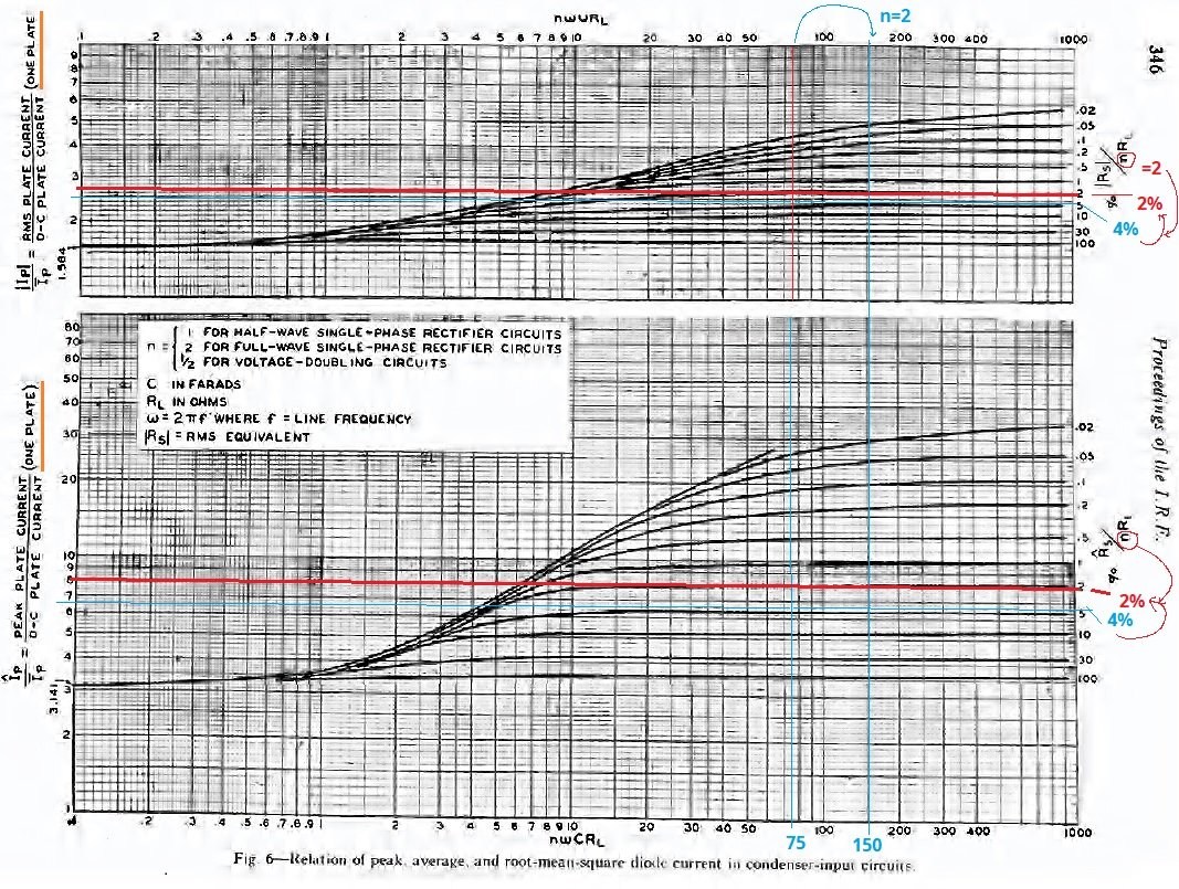
What we can see from the Schade's curves that we can't see easily from PSUDII, is that as Rs (the "equivalent" resistance) of the transformer/diode decreases, the Peak current and RMS current in the diodes and secondaries increase. I'm really grateful for PSUDII, it makes all of this easier to do and harder to mess up.
We can do some creative accounting on the transformer currents. If the HV secondary RMS current is running a little high, if we cut back on filament RMS currents we can help pay for that. It is not a perfect 1:1 trade. The trade for RMS currents is to keep the total power loss the same. This method starts to fall apart when the current used (I_used) gets to be more than about 15% higher than I_rated:
+ DCR sec_1 * I_rated Sec_1 ^2
+ DCR sec_2 * I_rated Sec_2 ^2
+ DCR primary * I_rated Primary ^2
The above is greater than or equal to:
+ DCR sec_1 * I_used Sec_1 ^2
+ DCR sec_2 * I_used Sec_2 ^2
+ DCR primary * I_used Primary ^2
-
From the Table below, we'll see that the Bias capacitor's DC voltage rating and PWB spacing dominate the design risk for allowed voltage. The Bias capacitor impacts the design multiple times.
1. The allowed DC voltage, closely followed by the allowed AC voltage, limits the allowed Vrms.
2. The value of the capacitor impacts the transient peak power and steady state RMS power pushed into the damping resistors.
3. As discussed above, the Bias capacitor impacts how bright the LED can be and how low in input voltage we can run.
The pad to pad voltage spacing under the diodes is also one of the voltage limits. A larger board would be needed to fix this issue.
| Common Assumptions |
1.15
Rise High line / Nominal |
1.1
Rise At no load |
Shade Factor of 1 (i.e. no load) | No bonus from Soft Start Resistor | Cbias
+ Rbias Damps out Turn On V Spike |
| Part
Rating Limitation |
Rule | FWB
Vpkpk limit On full winding |
FWCT
Vpk limit On half winding |
FWB Vrms Allowed Nominal Line Full Winding |
FWCT Vrms Allowed Nominal Line Half Winding |
Risk If exceeded Short term 5=High |
| 1200Vpk MOSFET | 1)
Vds 1200V
rating not
exceeded at
turn on. 2) V top Anode to ground < V_part |
1200.0 | 1200.0 | 670.8 | 670.8 | 5 |
| 1600V DC Cap | Peak
voltage = DC
Rated 1) Vout unloaded FWB 2) 2X Vout unloaded FWCT |
1600.0 | 800.0 | 894.4 | 447.2 | 4 |
| 2000V DC Cap | Peak
voltage = DC
Rated 1) Vout unloaded FWB 2) 2X Vout unloaded FWCT |
2000.0 | 1000.0 | 1118.0 | 559.0 | 4 |
| 650V AC Cap | Vrms
rated = 1) 0.5 times Vrms FWB 1) 1.0 times Vrms FWB |
1838.5 | 919.2 | 1027.7 | 513.8 | 4 |
| 700V AC Cap | 1)
Vrms =
Vpkpk/2/sqrt(2) 2) Vrms = Vend to end/2 |
1979.9 | 989.9 | 1106.7 | 553.4 | 4 |
| 2000Vpk*0.9
Diodes Diodes Matched Same Supplier Lot |
Anode-Anode Peak voltage < DC Rated 1) Vout unloaded FWB 2) 2X Vout unloaded FWCT |
1800.0 | 900.0 | 1006.2 | 503.1 | 5 |
| 1600V
PWB Coated Weak Spot Spacing Under Diodes |
Anode-Anode Peak voltage < Rated 1) Vout unloaded FWB 2) 2X Vout unloaded FWCT |
1600.0 | 800.0 | 894.4 | 447.2 | 4 |
| 1400Vpk
Across Bias Capacitor R_series ( < 200usec RC ) |
V across resistor < Pulse Vrating | 1400.0 | 1400.0 | 782.6 | 782.6 | 3 |
| Pulse
Power from
47nF into two 1K Resistors |
1)
Pulse Energy
< Rated
Pulse Joules 2) Pulse Rated Resistor used. |
900.0 | 900.0 | 503.1 | 503.1 | 3 |
| Min of above | 503.1 | 447.2 | ||||
| One
Leg => For the line above |
251.5 | 894.4 | <=End-End For the Line above |
| Change from 47nF to 68nF capacitor. | ||||||
| Pulse
Power from 68nF into two 1K Resistors |
1) Pulse Energy <
Rated Pulse Joules 2) Pulse Rated Resistor used. |
850.0 | 850.0 | 475.1 | 475.1 | 3 |
| Min of above | 475.1 | 447.2 | ||||
| One Leg => For the line above |
237.6 | 894.4 | <=End-End For the Line above |
|||
| Change from 47nF to 33nF 2kV 700Vac capacitor. | ||||||
| Pulse
Power from 33nF into two 1K Resistors |
1) Pulse Energy <
Rated Pulse Joules 2) Pulse Rated Resistor used. |
989.0 | 989.0 | 552.8 | 552.8 | 3 |
| Min of above | 552.8 | 447.2 | ||||
| One Leg => For the line above |
276.4 | 894.4 | <=End-End For the Line above |
|||
The table above assumes that the secondary voltage listed are given at 115Vrms input and the wall socket varies from 105 to 132Vrms. The table also assumes the secondary voltage will rise 10% when it is unloaded.
There is no additional
margin in the numbers above. I recommend that if the
table limited us to 447Vrms secondary voltage, we
use it at a voltage lower than that, 20% or more
lower. A surge
to 132V is not really a surge, it is
just high line. However, with
a "multiple line cycle" surge to
158Vrms (+20%) on the 115V, I'd be
willing to push the margins on PWB
spacing and Pulse ratings into the
Rbias resistors. I would not push
the voltage rating for any of the
diodes or FETs.
We can also buy additional margin by
1. Spending two times $2 more ($4) and buy the 2000Vdc 650Vac rated 47nF capacitor.
2. Thinning the conformal coat with solvent and applying it to the SMB diodes to force it under the diodes, letting it dry and then applying a thicker coat over then entire PWB.
Switching to a 800V FET or 800V SMB input diodes is a bad idea. Both of these parts are likely to see some unexpected "abuse" in use and we'll want the additional margin in our pockets.
If I were using a larger PWB, I'd
A. Switch to larger SMC diodes, possibly 3 of them
B. Use three 1210 resistors in series in the Cbias damping network or add in a circuit that keeps the "RUN FET (GATE2)" from turning on if there is more than ~200V across the soft start resistor.
The 33nF bias caps are rated for 700Vrms and 2000Vdc (Vpk). This is with no margin and must be respected at no load and at high line. High line is normally 132V steady state on the 120V/115V line. If we get a surge to 180Vrms, many electrical things are going to break, so this circuit may just be another one of them if we don't add extra padding. 132V/115V is a 1.15:1 ratio.
Typically the output voltage of a medium size HV tranformer rises 10% at no load. I've seen more than 20% on a low power cheap transformer, but the ones from Hammond run 10% or lower.
In worst case operation, the bias capacitor's ratings would be met at 2000Vdc (i.e. the unloaded output voltage at high line) with one lead at 1000Vdc and and the other lead referenced to a ground referenced 700Vac (+/- 1000Vpk). The first lead sees zero to -2000V peak. The other lead sees +/- 1000Vpk or 700Vrms. This yeilds 2000Vpk and 700Vrms stress on the part.
The higher output power Hammond power transformers I checked are specified at 115Vrms input and have about a 10% no load to full load regulation. With the 700Vrms ratings on the 0.033uF capacitors, this says the power transformer's nominal datasheet output can be rated for
700Vrms * 115V nominal /132V high line / 1.10 regulation factor = 553Vrms/leg with a 115V Primary fed by 115V nominal.
A capacitor rated for 2000Vdc, 650Vac would need a transformer nominally specified at
650Vrms * 115V/ 132V line variation / 1.1 regulation = 513.8Vrms/leg with a 115V Primary fed by 115V nominal.
The 132Vrms high line isn't unrealistic, I have measured 135Vrms on the wall sockets in my home in the year 2000 time frame and 105Vrms at the wall sockets in the house I lived in during the 1990s (an old neighborhood.) So I'm being generous (maybe even foolhardy) with the low upper limit of 132Vrms.
For the bias capacitors ratings, this 553Vac becomes 1106Vrms_ct (1564Vpkpk.) The transformers used should say 553V-0-553V or lower. With respect to the capacitor alone, this rating holds for full wave center tap or full wave bridge. However, this 1106Vrms can't be used when using a full wave bridge because of the 1200V FETs. The caps will survive, but the 1200V FET will not.
At first power-up, I'd use the 125V taps on the transformer with the 115V tap "capped off." If I needed a bit more output voltage because my line voltage was low, I'd use the 115V input and then cap and restrain the 125V lead from the transformer.
At turn-on, the FET will see the full peak unloaded voltage from the transformer.
Some low power transformers have a worse regulation factor (>1.2:1 vs 1.1:1) which will require using an even lower voltage rated transformer. The Hammond 263X runs a no load voltage of 1.02*222.9/200 -1 = +13.7%. This part is not a "bad" design. This is a lower voltage transformer so a slightly larger regulation factor isn't an issue. When we hit 553-0-553V transformers, it is an issue. The higher no-load voltages is the nature of the beast for low VA, temperature rise limited transformers designs. Lowell Quist published a paper on how to design regulation limited transformer designs Lowell Quist on regulation limited transformer designs, see equation 17. Paul extended this method to inductors. DCR limited Inductor Design
FETs do not have much design margin on their breakdown voltage. In the 1990s, one manufacturer told me that they only had one sigma margin between the data sheet rating and the actual shipped performance after I contacted them about parts not meeting the datasheet voltage rating values. This means they easily could be shipping parts that did not meet datasheet requirements. No I will not name them. They seem to have learned a bit about "Design for 6 Sigma" in the intervening years, and that part is no longer being sold. The older part I questioned was randomly failing during voltage surges, it was not failing in normal operation. Newer parts from that company are behaving acceptably.
The 1200V FET will only support
1200V/1.15 line reg/1.1 secondary reg/sqrt(2) = 670Vrms (335-0-335) in full wave bridge or (670-0-670V) in full wave center tap.
Remember that the capacitor's rating will limit us to using a lower voltage of (553V-0-553V) in full wave center tap. At 670Vac with an O.H. Shade figure of merit of 0.85, this will result in an 806Vdc output with a full wave bridge (two 2000V diodes added externally.) With a full wave center tap, the 1200V FET can take 670V-0-670V, but the capacitor limits the voltage to be 553-0-553Vrms. With the same O.H. Shade figure of merit, the full wave center tap (1106Vrms_ct or 553V-0-553V) will generate a 664Vdc output. Alas, other parts will limit us to using lower Vrms inputs.
A less expensive 800V FET will only support 800V/1.15 line reg/1.1 secondary reg/sqrt(2) = 447Vrms (223-0-223) in full wave bridge. With an O.H. Shade figure of merit of 0.85, this will result in a 537Vdc output with a full wave bridge (two 2000V diodes added externally.) With a full wave center tap, the 800V FET can take 447V-0-447V. The capacitor is not the limiting factor this time. With the same O.H. Shade figure of merit, the full wave center tap (894Vrms_ct or 447V-0-447V) will generate a 537Vdc output (with ZERO DESIGN MARGIN for line transients and other overshoots.)
Note: 447Vrms * 1.15 line regulation * 1.1 = 565.5Vrms high line unloaded. If 447Vrms is the limiting voltage on the design, we could drop from a 700Vac rated film capacitor to a 600Vac rated one. It could save $0.58 on each cap and the cap could be 0.13" shorter.
Absolute Maximum Ratings with the less expensive 800V MOSFET
With respect to this effort, if we want to get to a 1200V output (211 voltages), we'll need a bigger board, bigger MOSFETs, likely a 1700V SiC leaded TO-247 part and higher voltage input diodes and bias capacitors. I can only find one surface mount D3PAK that has a chance of working in this design, whereas I can find multiple TO-247 parts and the TO-247 parts cost less. I'd use the TO-247 parts. I'd still use surface mount for the timers. However, for 1200V output, I think I'd rather move the soft start to the primary side of the transformer and use a separate filament transformer for the heaters.
This is a trick question.
The diodes are rated at 1000V breakdown, so
two perfectly matched parts in series should
allow for a best case 2000V rating from
cathode to anode. BUT. the pad
to pad spacing for the SMB package diodes
is only 70 mils. With a clean board
and conformal coat, IPC B4 will allow 800V
peak across the diodes. The spacing rule
that I trust (Old Eng Rule) for coated
boards will only allow 600V peak.
Switching to SMC diodes will fix this
issue, but to fit these parts the board
gets a lot wider and longer. I'd really
like to fit this design in my Dynaco FM3
tuner. So on this version, I'll take a
hit and risk on the PIV and later we'll
spin a board that will use SMC diodes.
It
looks like the part will still solder
down with 80 mil pad to pad spacings so
I'll change the layout to 80 mils and
allow 800V per diode.
Remember that the diodes see the end to end voltage coming out of the transformer. With a full wave center tap, this Anode to Anode peak to peak voltage is twice the voltage rating for one leg. At power-up the FET will see a peak voltage equal to the Vrms rated for 115V input * 1.15 * 1.1 * sqrt(2) = 1.79 * Vrms. The diodes see twice this for 3.58 * Vrms with respect to the Vrms-0-Vrms rating. With 553Vrms/leg, at initial power-up, this is 1980Vpeak at the Anode to Anode design point.
During
normal operation, high line, the diodes
will see steady state approximately
[ 1 (the peak loaded winding) + 1/0.85
Shade factor for the unloaded winding
] *1.15 high line = 2.5 times the DC
output voltage
with respect to normal loaded operation. But this is not the design point for part stress. However, it is a number that buys us margin for voltage surges during operation. The diodes have to survive at turn-on where the voltage from the transformer rises.
Back to the question at hand
Let's round the sharp corners on the diode lands and take a risk and use the IPC B4 rating for a PIV of 1600V (we'll still use the 1000V diodes because the board may survive a transient above 800V, the diodes won't. For unloaded power-up at high line:
1600V
/ 1.15 for high line / 1.1 for
unloaded voltage rise / sqrt(2) =
1265V/sqrt(2) =
894Vrms when used as a full wave bridge
(447V-0-447V) for Full Wave CT..
894Vrms for full wave bridge is higher than what the FET ratings allow for so the diodes are not the limiting factor in "FW BRIDGE" operation. If we drop to a 600V rating across each diode (1200Vpk) we actually have the same ratings as for a 1200V FET. (Already, I'm feeling better that I'm doing the maths right.)
With the 800V per diode, this drops to (447V-0-447V) with 115V input when the secondary is used as a full wave center tap. This is lower than what the FET can take (670-0-670) and is lower than what the capacitor can take (553-0-553) and thus limits our design. The (447V-0-447V) with a full wave center tap and an OH Shade factor of 0.85 gets us 447V*sqrt(2)*0.85 = 537.5V dc (not counting Diode drops and High Voltage filtering drops).
The diodes would have to support 1600Vpk * 553V/447V = 1979Vpk to make the 1200V FET the limiting factor. The spacing on SMC diodes will support this voltage, but SMC is a lot bigger than SMD diodes and I'm already not fully happy with how big this PBA is. If we limit the Full Wave CT to (447V-0-447V) we could also drop the film capacitor's rating from 700Vac to 600Vac and save a little room and a little money.



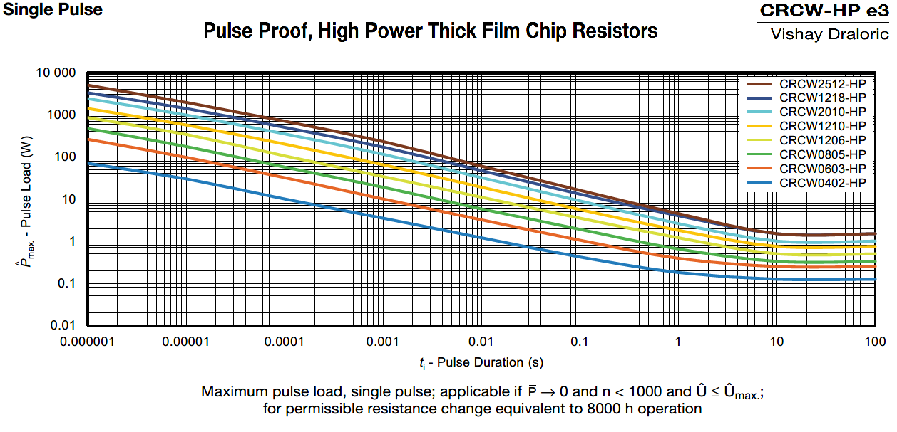 ..
..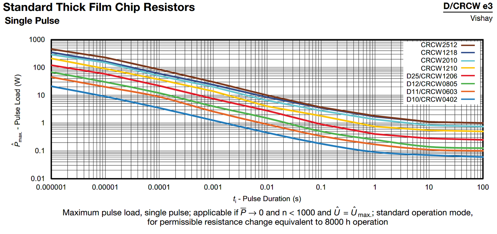
| Time (usec) | 1X Standard Resistor |
1X Pulse Rated Resistor |
1X Standard Resistor |
1X Pulse Rated Resistor |
1X Pulse Rated Resistor Min Ohm |
Max nF Cap 2 Res in series Pulse Rated R |
2X Pulse Rated | Max R (1x) at
0.4W Cap +10% 60 Hz Vrms max = |
Max R For an RC of 1.66msec (1/60Hz/2/5) |
Steady State Loss Check < 0.4W per R |
| Square Pulse | Square Pulse Watts |
Square Pulse Watts |
milliJoules | milliJoules | at 450Vpk | at 900Vpk total | RC usec | 636 | ||
| 7.3 | 100 | 670 | 0.73 | 4.89 | 302.2 | 24.2 | 14.6 | 9844.9 | 114685.1 | OK |
| 20.0 | 68 | 420 | 1.36 | 8.40 | 482.1 | 41.5 | 40.0 | 3337.7 | 66776.8 | OK |
| 35.0 | 57 | 330 | 2.00 | 11.55 | 613.6 | 57.0 | 70.0 | 1765.4 | 48564.9 | OK |
| 40.0 | 52 | 310 | 2.08 | 12.40 | 653.2 | 61.2 | 80.0 | 1531.7 | 45235.9 | OK |
| 70.0 | 43 | 240 | 3.01 | 16.80 | 843.8 | 83.0 | 140.0 | 834.4 | 33388.4 | Can't use |
| 100.0 | 38 | 210 | 3.80 | 21.00 | 964.3 | 103.7 | 200.0 | 534.0 | 26710.7 | Can't use |
| 200.0 | 28 | 140 | 5.60 | 28.00 | 1446.4 | 138.3 | 400.0 | 300.4 | 20033.0 | Can't use |
| 47nF 2000V 700Vac capacitor | ||||||||
| nF cap | Vpk Max | Nom. MilliJoules | 1R Ohms | 1R pk Watts |
2R RC usec | 1R allowed Watts At 2RC |
1R Rated At 1RC Watts |
Note |
| 47.0 | 900 | 19.0 | 641 | 315.9 | 60.3 | 262.6 | 318.0 | Overstressed |
| 47.0 | 900 | 19.0 | 1000 | 202.5 | 94.0 | 216.0 | 293.7 | Increase R |
| 47.0 | 928 | 20.2 | 1000 | 215.3 | 94.0 | 216.0 | 293.7 | Check Vpk margin |
| Change to 68nF 1600V 650Vac capacitor | ||||||||
| 68.0 | 900 | 27.5 | 1000 | 202.5 | 136 | 184.8 | Skip calculation | Change Cap, Same Vpk |
| 68.0 | 850 | 25.1 | 1000 | 180.6 | 136 | 184.8 | Skip calculation | Decrease Vpp to pass |
On the other end of the calculations, if we didn't get any help from the LED and the LED voltage were to climb to 11.3V + 0.62V (designer's choice) because of low Hfe, the protection cap would have to be (solving with charge, Q = C*V)
Minimum cap = 1200V * 0.033uF/11.92V = 3.32uF
Nom value X7R = 3.32uF / 0.9 tol / 0.80 age / 1 for room temperature = 4.6uF (a 10uF would work.)

For the Soft-Start Gate1 FET position, as long as the IGBT:
Turns on to about 1 amp at a reasonably low gate voltage (closer to 6V than 8V) we can use the cheaper IGBT.
Is not thermally stressed during turn-on
The SOA during turn-on isn't violated
After running the LTSPICE model at 15C and 85C, it shows we can use the IGBT. There are a couple 1200V IGBTs that meet this criteria so I'll switch over to them. The IGBT that are "current protected" sometimes have a higher Vgs turn-on voltage and won't work in this circuit.
For the RUN Gate2 FET position, as long as the IGBT:
Turns on to about 5 amp at a reasonably low gate voltage (closer to 6V than 8V) we can use the cheaper IGBT.
Is not thermally stressed during turn-on
Is less than about 1.5V Vds at 1.26A
The SOA during turn-on isn't violated.
The IGBT has an internal diode from drain to source (not all of them do.)
and the reversal of voltage across the part doesn't generate excessive noise.
After running the LTSPICE model at 15C and 85C, we should be able to use the IGBT. There are a couple 1200V IGBTs that meet this criteria except for the noise risk. The IGBT is about $7 cheaper than the FET. I think it is worth trying..There are a few short circuit protected IGBTs that won't work because the required gate drive voltage is too high.
The
STGB3NC120HD
meets all of
our
requirements
and only costs
$2.31 in 1 pc
quantities.
The first issue is failures from micro-cracks in the ceramic body of the capacitor.
I normally start to see SMT capacitors crack from mechanical strain occur at the 1210 size. The 1210's do require a bit of effort to break, such as snapping a PBA out of its carrier instead of cutting the carrier off. I have a friend who has had issues with SMT caps larger than 1812 because of cracking/crazing from temperature cycling. (i.e. 1825 doesn't work; but 1812 passes.)
A second related issue is violent failures.
I've personally had stacked ceramics "explode" in high current circuits because the surface cracked and the crack generated a short. If I didn't have PPE on, I would have been hurt. Ceramic caps with high CV products have thin dielectric layers that break easily in soldering and handling. Some of the new high CV product capacitors have very thin ceramic layers. They even crack from the thermal shock of soldering. Avoid the SMT ceramics with low voltage ratings because of this increase in cracking risk. Usually, if the part is rated for automotive use, it is lower risk than the same foot print part and value that is for general use. A coated ceramic X7R is lower risk because the surfaces are protected; the risk is still there, it is just many times lower.
A third issue is value drift on Class 2 ceramics ( X7R drifts, NPO does not.)
The temperature variation in X7Rs capacitor value is large. There also is a drop in capacitor value with DC bias. Then there is a 4-8% drop in value per decade hour of existence. i.e. 8% * log10 (hours of existence, powered or not.) The high CV product parts tend to run closer to the 8% change, the older CK05/CK06 military ceramics and commercial parts of same size tend to run closer to the 4% change. -8% * log10(10 years * 8000hr/yr) = -39.2% (-44% change in value occurs in 39 years) These three issues are additive. A 10% change from temperature plus 20% drop from DC bias plus 40% drop from aging says we only have 30% of the original value left.
This part drift with age is
real. My cube mate at work got bit
by it.
A fourth issue is self heating. NPO and N1500 capacitors don't have this issue. Self heating is the big issue with AC on X7R capacitors. The issue is that the capacitor gets hot.
From digikey, there are two
HV ceramics in 1812 (we won't even
consider the 1825 size parts). One
is a 0.1u 1kV 1812Y1K00104KST (Knowles/ Johanson MFG) and the other
is a 39nF 1812J1K50393KXT in
1500kV. Both over $3
each.
The pads for these run 96 mils apart which would make them closer to 860Vpk, 608Vrms best case parts.
From "AC Power Computations for DC Rated Capacitors" by Johanson Dielectrics the 1812 capacitor can handle 0.4W at 25C. At 85C this drops to (125-85C)/(125-25C) = 0.16W allowed. The dissipation curves below are from the same Johanson Dielectrics source.
| 1000V | %change value | %dissipation | Cap | Tol Cap | Freq | PWR | Scale Voltage by 0.16W |
| 100 | 35.00% | 12.00% | 1.00E-07 | 10.00% | 60 | 0.067 | 154 |
| 200 | 45.00% | 18.00% | 1.00E-07 | 10.00% | 60 | 0.433 | 122 |
| 400 | 10.00% | 4.00% | 1.00E-07 | 10.00% | 60 | 0.292 | 296 |
| 2000V | %change value | %dissipation | Cap | 10.00% | Freq | PWR | |
| 100 | 25.00% | 8.00% | 1.00E-07 | 10.00% | 60 | 0.041 | 196 |
| 200 | 35.00% | 14.00% | 1.00E-07 | 10.00% | 60 | 0.314 | 143 |
| 400 | 45.00% | 18.50% | 1.00E-07 | 10.00% | 60 | 1.780 | 120 |
| 100 | 25.00% | 8.00% | 3.90E-08 | 10.00% | 60 | 0.016 | 315 |
| 200 | 35.00% | 14.00% | 3.90E-08 | 10.00% | 60 | 0.122 | 229 |
| 400 | 45.00% | 18.50% | 3.90E-08 | 10.00% | 60 | 0.694 | 192 |
| Average 1k
2k For 1.5kV |
%change value | %dissipation | Cap | 10.00% | Freq | PWR | |
| 100 | 30.00% | 10.00% | 3.90E-08 | 10.00% | 60 | 0.021 | 276 |
| 200 | 40.00% | 16.00% | 3.90E-08 | 10.00% | 60 | 0.145 | 210 |
| 400 | 27.50% | 11.25% | 3.90E-08 | 10.00% | 60 | 0.371 | 263 |
This card must be clean of flux, oils and fingerprints. The board was designed to be first dried and then conformal coated before it is used. The drying can occur from a 60-80C bake out in a PLA filament dryer or wrap the PBA in foil and baked it at 70C (158F) sandwiched between two cooking pans in a toaster oven.
In the design, I'll follow the trace spacing from the "Old Engineer Rule" for spacing. This Old Engineer guide has been working for decades. I trust it more than IPC. I've had failures between traces closer than 10 mils (that was allowed by IPC) in the past at voltages as low as 15V, so the B1 spacing for use from IPC on power products are suspect in my book.
| . | Internal | External unCoated | External Coated | . | Internal + coated | Web Article | . | NAVSOP-4855-1A | NAVSOP-4855-1A | NAVSOP-4855-1A |
| IPC B1 | IPC B2 | IPC B4 | Old Eng Rule | 100V/mil | Para 4.1.1 | Para 4.1.1 | Para 4.1.1 | |||
| Vpk | mils | Mils | Mils | 10V/mil + 10mil | Layer to Layer | Layer-Layer 50V/mil | external DC 25V/mil | external AC 12.5V/mil | ||
| 2000 | 158 | 394 | 212 | 210 | 20 | 40 | 80 | 160 | ||
| 1200 | 79 | 236 | 116 | 130 | 12 | 24 | 48 | 96 | ||
| 1000 | 59 | 197 | 92 | 110 | 10 | 20 | 40 | 80 | ||
| 800 | 40 | 158 | 68 | 90 | 8 | 16 | 32 | 64 | ||
| 600 | 20 | 118 | 44 | 70 | 6 | 12 | 24 | 48 | ||
| 300 | 10 | 99 | 32 | 40 | 3 | 6 | 12 | 24 | ||
| 15 | 2 | 4 | 2 | 11.5 |
Here is the same table with dimension in mm instead of 1/1000 (mil) of an inch.
| . | Internal | External unCoated | External Coated | . | Internal + coated | Web Article | . | NAVSOP-4855-1A | NAVSOP-4855-1A | NAVSOP-4855-1A |
| IPC B1 | IPC B2 | IPC B4 | Old Eng Rule | 100V/mil | Para 4.1.1 | Para 4.1.1 | Para 4.1.1 | |||
| Vpk | mm | mm | mm | mm | mm | mm | mm | mm | ||
| 2000 | 6.22 | 15.51 | 8.35 | 8.27 | 0.79 | 1.57 | 3.15 | 6.30 | ||
| 1200 | 3.11 | 9.29 | 4.57 | 5.12 | 0.47 | 0.94 | 1.89 | 3.78 | ||
| 1000 | 2.32 | 7.76 | 3.62 | 4.33 | 0.39 | 0.79 | 1.57 | 3.15 | ||
| 800 | 1.57 | 6.22 | 2.68 | 3.54 | 0.31 | 0.63 | 1.26 | 2.52 | ||
| 600 | 0.79 | 4.65 | 1.73 | 2.76 | 0.24 | 0.47 | 0.94 | 1.89 | ||
| 300 | 0.39 | 3.90 | 1.26 | 1.57 | 0.12 | 0.24 | 0.47 | 0.94 | ||
| 15 | 0.08 | 0.16 | 0.08 | 0.45 |
Trace Widths for 1A RMS:
| 0.5 Oz CU 1 Oz plate 5C rise |
1 OZ 5C Rise |
0.5 Oz CU 1 Oz plate 5C rise |
1 OZ 5C Rise |
||
| A rms | External mil | Internal mil | External mm | Internal mm | |
| 1 | 16 | 24 | 0.63 | 0.94 | |
| 1 Sec Fusing | 1 Sec Fusing | ||||
| 5.0 Arms | 5.5 Arms |
Remember:
Any traces with more than 200Vpk between them should consider rounded corners on both the low voltage and high voltage sides. 270Vpk at 60Hz is the Paschen minimum for air. The Paschen minimum is the lowest voltage where air breakdown can start. It doesn't mean that breakdown occurs, it means that it can occur. At higher frequencies, the Paschen minimum voltage drops. Solder mask doesn't remove the risk, but it does help keep the effective board surfaces cleaner.
Any traces with more than 450Vpk between them, need rounded corners. I've measured air going into corona at 325Vrms (459Vpk) at room pressure.
There should be no square
pads facing each other between
high and low voltage. One fix is
to used rounded guard traces.
Guard traces on the outer layers
work better than guard planes on
inner layers, but If you can't fit
the trace on the outer layer, make
sure you but a rounded edge guard
plain/trace on an inner
layer. Another fix is to put
rounded edges on the square pads.
We have to avoid sharp points when using high voltage. This sharp point rule is in 3D, not just in the X and Y dimensions. Corona and voltage break down issues are real. I've had to fix them in production. If you are in between a rock and a hard place on making things fit, trading a little more (not a lot) of corona risk during turn-on vs lower corona risk in normal operation is the correct choice. That does NOT mean you can use 32 mil trace spacing at 800V (unloaded) peak (should be 90mil) to pass turn-on stresses.
From the PGE 120V Voltage Specs the NEMA line voltage range is 103.5 to 126.5. Other specs I've found quote 132Vrms as the maximum for a 120V line. Some time ago, I had 132Vrms every day at my house with long durations of 135V. Light bulbs didn't last long. This is likely because the utility's step down transformer for the neighborhood literally was in my front yard. My house runs high on voltage so the neighbors at the end of the longest wire from the step down transformer get a voltage that isn't too low.
I've seen surge suppressor strips (bigger ones, not the low price simple ones) list a 150Vrms "equivalent" clamp voltage which I assume to mean that the normal 120Vrms peak of 170Vpk is limited to 212Vpk at the "specified current." 150Vrms is a line voltage that is 30% higher than 115Vrms. In this article, I planned on +15% (132Vrms) for high line. This would indicate we should reduce the allowed secondary voltage by 15%, preferably 20%, to provide margin for transients. Before you say Solid State is junk, this same margin should also be applied to tube rectifiers.
115Vrms is used as nominal in these pages because many of the Hammond line transformers have 115V/230V primaries. If your wall socket is 125V, use the 125V winding on the Hammond Transformer and "cap off" and restrain the 115V lead.
The biggest risk for failure from a voltage surge in this design is during the 18 and a half second delay before turning on the RUN MOSFET (IGBT). During this time the rectifier is high impedance and provides no filtering for spikes and surges. Once the RUN MOSFET (Gate 2) is switched on, the output capacitors work against the leakage inductance and effective DCR of the power transformer to pull the voltage surges down. From the PGE document, we can see what the effective transient voltages and durations will be:
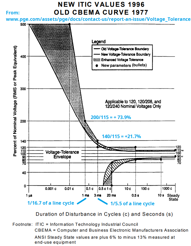
140Vrms
on a 115Vrms
line takes
a 447Vrms
output from
632Vpk loaded
to
770Vpk
(loaded),
847Vpk
(+10%
unloaded) per
leg.
We
have a decent
chance of
surviving this
one in the
first 18
seconds if we
drop the
transformer
from 447Vrms
to
422Vrms.
Nothing else
is required.
However, more
protection is
always
"Desired."
In
normal
operation with
the Run MOSFET
on, I modeled
these 1msec
and 3msec
"short" surges
in LTSPICE. I
guessed at the
leakage
inductance of
the HV
secondary as
1mH. In the
model, a
voltage pulse
with a
controlled
rise and fall
time was the
easiest to
use. If you
try to set
this up with a
sinewave with
a "phase
shift", the
sine generator
will output a
DC voltage,
not zero
volts, until
the pulse
begins. Below
is the pulse
generator I
used.
.
The first transient occurring at 104msec is the 3 msec wide +21.7% transient. The second transient at 404msec is the 1msec wide +73.9% transient. When the line transient pulse occurs with the regulator in the "RUN" mode, the output cap works against the leakage inductance and series resistance of the high voltage secondary to pull the pulse voltage down far enough that the design will be in good shape. Less than a 10% rise in the output voltage and we just have to push the PWB voltage rating a little bit.
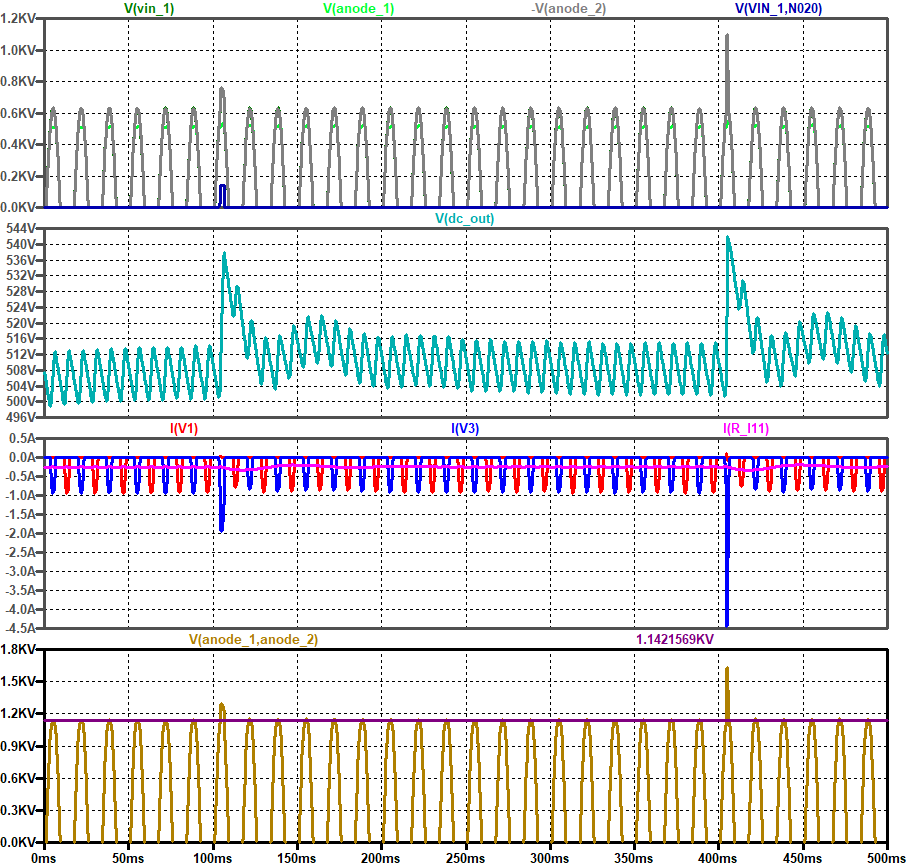
If you really need more protection, put four series 1.5kW to 30kW bi-directional TVS between Anode_1 and Anode_2. These parts will need to be sleeved with flame resistant heatshrink. If we use the 1.5KE350CA TVS at $0.60 each and let the part stresses between Anode_1 to Anode_2 run at almost 2kV, we have some protection during the first 18 seconds. We'll have to push the stress on the board's trace spacing a little, but that may be acceptable because this is a short term stress, not long term. We'll also want to use the high voltage rated 47nF capacitor and the 1200V MOSFET/IGBT.
We'll also have to limit the transformer secondary to be less than or equal to 371Vrms-0-371Vrms at 115V input to keep from overheating the stack of four TVS diodes.


-
In the appendices below I'm opening my notebook further for people who want nit pick the design. . .
Time to discharge desired = T1
Delay time before discharge starts = Td
Maximum initial voltage on capacitor = Vstart
Rnom discharge = (T1 - Td)/[-ln(50V/Vstart)]/(1+Cap tol)/(1+res tol)/Cnominal (farads)
If
we just want to meet the NEC
60 second/5 minute limits
with reasonable cap sizes,
throwing away 2 watts of
loss (a 5W resistor) in the
bleeder resistor isn't that
bad. When the capacitors get
BIG or we don't want to wait
a long time, then the
bleeder resistors get to be
a challenge if they are
always attached to the high
voltage rail. This
capacitor energy storage
issue exists whether you are
using tube or solid state
parts.
|
Voltage |
uF |
Cap |
Joules |
Time |
Trigger |
Res |
Resistor |
Resistor |
Comment |
|
51 |
64078.0 |
20% |
100.00 |
60 |
0.50 |
5.0% |
37.2 |
0.07 |
100J Just over 50V |
|
100 |
16666.6 |
20% |
100.00 |
60 |
0.50 |
5.0% |
4.09 |
2.57 |
100J Limit at 100V |
|
101 |
163.3 |
20% |
1.00 |
60 |
0.50 |
5.0% |
411.3 |
0.03 |
1.0J Limit start point |
|
250 |
26.6 |
20% |
1.00 |
60 |
0.50 |
5.0% |
1103.0 |
0.06 |
|
|
399 |
10.5 |
20% |
1.00 |
60 |
0.50 |
5.0% |
2171.8 |
0.08 |
|
|
400 |
10.4 |
20% |
1.00 |
60 |
0.50 |
5.0% |
2180.0 |
0.08 |
|
|
401 |
2.6 |
20% |
0.25 |
60 |
0.50 |
5.0% |
8453.2 |
0.02 |
0.25J Limit start point |
|
600 |
1.2 |
20% |
0.25 |
60 |
0.50 |
5.0% |
16419.2 |
0.02 |
60 sec upper limit |
|
601 |
1.2 |
20% |
0.25 |
300 |
0.50 |
5.0% |
82864.8 |
0.00 |
300 sec lower limit |
|
250 |
364.7 |
20% |
13.68 |
60 |
0.50 |
5.0% |
80.5 |
0.82 |
one of my designs |
|
540 |
154.0 |
20% |
26.94 |
60 |
0.50 |
5.0% |
128.9 |
2.38 |
Another design |
|
540 |
154.0 |
20% |
26.94 |
10 |
0.50 |
5.0% |
20.6 |
14.88 |
|
|
540 |
154.0 |
20% |
26.94 |
19 |
0.50 |
5.0% |
40.1 |
7.64 |
|
|
540 |
256.0 |
20% |
44.79 |
16 |
0.50 |
5.0% |
20.2 |
15.16 |
|
|
540 |
1001.0 |
20% |
175.13 |
60 |
0.50 |
5.0% |
19.8 |
15.44 |
|
|
720 |
154.0 |
20% |
47.90 |
300 |
0.50 |
5.0% |
578.7 |
0.94 |
Another design |
|
720 |
154.0 |
20% |
47.90 |
15 |
0.50 |
5.0% |
28.0 |
19.43 |
|
|
720 |
256.0 |
20% |
79.63 |
10 |
0.50 |
5.0% |
11.0 |
49.29 |
|
|
720 |
256.0 |
20% |
79.63 |
24 |
0.50 |
5.0% |
27.3 |
19.93 |
|
|
800 |
154.0 |
20% |
59.14 |
22 |
0.50 |
5.0% |
40.0 |
16.82 |
|
| Total Capacitance for the 100 Joule Limit | |||||
| Vnom | Vhigh line (+15%) |
Vno Load (+10%) |
Max Cap (at +10%) |
Nom Cap | Nom uF |
| 100 | 115 | 126.5 | 1.25E-02 | 1.14E-02 | 11362 |
| 200 | 230 | 253.0 | 3.12E-03 | 2.84E-03 | 2841 |
| 300 | 345 | 379.5 | 1.39E-03 | 1.26E-03 | 1262 |
| 400 | 460 | 506.0 | 7.81E-04 | 7.10E-04 | 710 |
| 500 | 575 | 632.5 | 5.00E-04 | 4.54E-04 | 454 |
| 600 | 690 | 759.0 | 3.47E-04 | 3.16E-04 | 316 |
| 700 | 805 | 885.5 | 2.55E-04 | 2.32E-04 | 232 |
| 800 | 920 | 1012.0 | 1.95E-04 | 1.78E-04 | 178 |
| 900 | 1035 | 1138.5 | 1.54E-04 | 1.40E-04 | 140 |
| 1000 | 1150 | 1265.0 | 1.25E-04 | 1.14E-04 | 114 |
| 1100 | 1265 | 1391.5 | 1.03E-04 | 9.39E-05 | 94 |
| 1200 | 1380 | 1518.0 | 8.68E-05 | 7.89E-05 | 79 |
On the 1 amp curve, at 1 second the the fuse clears at about 2.25 Amps. At 20msec, the fuse clears at about4.0 Amps.
At high line, over a 20msec window, we'd want the RMS current to be less than 3 amps (405VA at 135V) so we have some margin on the fuse's ratings.
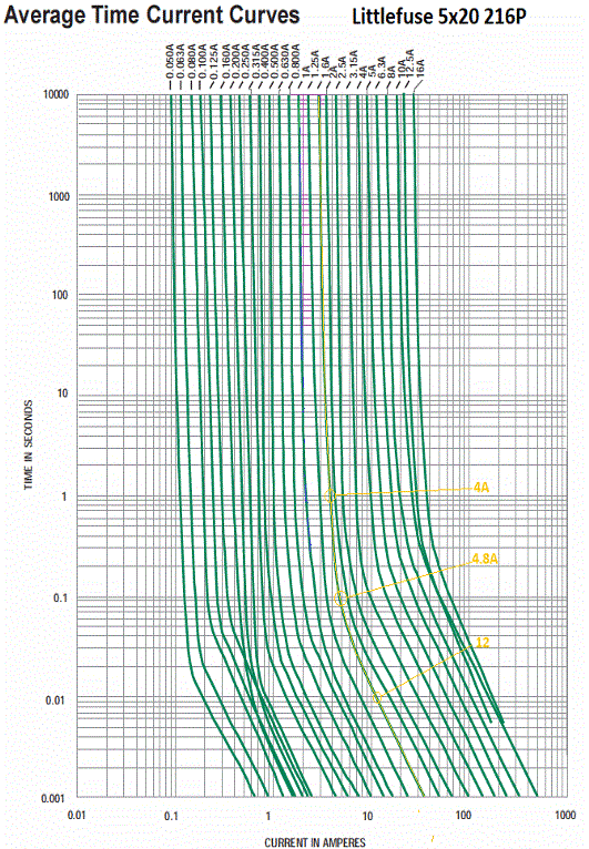
To reflect power on the secondary of the transformer to the primary, keep the power the same and work the math with the equivalent primary voltage. After solving for nominal, linearly scale the 115V input results to high line voltage.
400Vrms * 0.135mA = 54W.
54W/115V = 0.470A.
After solving for nominal, linearly scale the 115V input results to high line voltage.
Increasing
to 132V
input:
0.47A *
132V/115V =
0.54A
On the SMT parts, use water or IPA soluble flux on every solder joint before the iron touches the board. This isn't the flux inside the core of the solder. This is flux you apply yourself through a small bottle.
After soldering, clean the PBA after soldering! 90% IPA works nicely, but clean it outside. 90% IPA is flammable, 70%, not so much. Clean even with no-clean fluxes. This is high voltage and is something we want to last 20 years, not to the end of a 30 day warranty. Some capacitors do not like being submerged in solvents: Carbon Comp resistors, Aluminum capacitors, non-hermetic Tantalum capacitors and some film capacitors. To be safe, super clean the board before putting on the film capacitors and then give it another cleaning before you conformal coat the PBA. (Printed Board Assembly)
From
Hammond
Transformers
and Inductors
5c. Individual
part data
taken directly
from each
individual
part's print.
| Part No. | VA | Primary | (R.M.S.) | AC From |
Secondary End to End No load |
Total Reflected Secondary DCR | Unloaded / Loaded | No
Load High Line (135) FWB |
Vout
dc Estimate FWB |
Vout
dc Estimate FWCT |
|
| VAC | Hz. | Vrms | mA | Vrms | Ohm | Percent |
Vpk |
Vdc | Vdc | ||
| 263AX | 32 | 115 | 60 | 100-0-100 | 115 | 222.9 | 157.23 | 110.3% | 370.05 | 261.94 | 130.97 |
| 269AX | 40 | 115 | 60 | 125-0-125 | 115 | 284.7 | 198.82 | 110.2% | 472.65 | 336.23 | 168.12 |
| 269BX | 38 | 115 | 60 | 150-0-150 | 86 | 337.8 | 276.51 | 109.0% | 560.80 | 400.06 | 200.03 |
| 263CX | 116 | 115 | 60 | 180-0-180 | 287 | 392.3 | 62.53 | 105.1% | 651.28 | 465.58 | 232.79 |
| 269GX | 48 | 115 | 60 | 225-0-225 | 75 | 507.5 | 502.43 | 109.4% | 842.53 | 604.06 | 302.03 |
| 270EX | 118 | 115 | 60 | 275-0-275 | 144 | 598.0 | 167.59 | 105.0% | 992.78 | 712.84 | 356.42 |
| 273BX | 182 | 115 | 60 | 350-0-350 | 201 | 791.0 | 140.11 | 104.2% | 1313.19 | 944.85 | 472.42 |
| 278CX | 454 | 115 | 60 | 400-0-400 | 535 | 841.7 | 41.87 | 102.8% | 1397.36 | 1005.79 | 502.90 |
| 282X | 273 | 115 | 60 | 500-0-500 | 230 | 1071.7 | 192.63 | 104.7% | 1779.20 | 1282.27 | 641.14 |
These are the settings I use in xCHECK when I check the ExpressPCB files. I avoid small holes and I allows small pads so I can use a small pad to put rounded corners on square cornered SMT pads.:
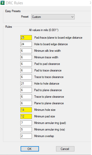
Choke input power supplies have several advantages over capacitor input designs. The biggest being that the current into the output capacitor is continuous and not peaked like capacitive input designs. The smoothed secondary current flow reduces the VA required by the transformer, for the same size transformer reduces the heating in the transformer and rectifiers , reduces the radiated noise from the leakage inductance of the power transformer and reduces the voltage noise induced into the primary winding of the transformer when compared to capacitive input designs. This last item can be important to amplifiers that use the same power transformer for the filaments as they do for the high voltage. Voltage distortion on the primary winding's DCR from the high voltage output's secondary current will induce voltage distortion on the filament windings. This distortion, AKA noise, is coupled to the cathode and/or grid and has a good chance of making it to the output of the amplifier. Another way to see this is that if the HV secondary current makes 5% voltage ripple on the primary winding from the DCR etc., of the primary winding, all output windings from that transformer will see this 5% distortion.
The
leakage
inductance of
the
transformer
radiates
energy from
the current
flow in the
windings.
The field is
often weakest
on the iron
side of the
transformer
and strongest
on the winding
side. Toroidal
transformers
can reduce
this issue,
but they do
not eliminate
it. The
voltage
induced by
this field is
proportional
to the "M" *
"di/dt" of the
current flow.
Where "M" is
the mutual
inductance
between the
noise source
and the
"victim"
circuit and
"di/dt" is the
rate of change
of current in
the windings.
A good choke
input design
will have a
lower "di/dt"
than a
capacitive
input design.
The little
glitch when
the current
transfers from
one winding to
another often
seems to not
be an issue,
and that
glitch can be
reduced if
needed (how,
that is
another very
long and
tedious
article).
The
internal
energy storage
on the control
circuit should
provide enough
turn off delay
to allow use
with a choke
input design
that
experiences
"reasonably
clean" 115V
power shut
off. (i.e. the
switch bounce
decays after 1
complete power
cycle.)
Below is a
typical Full
Wave Center
Tap Choke
Input
design.
For Choke
input designs,
I prefer a
Full Wave
Bridge because
it reduces the
risk of damage
from the 115V
switch off
spike.
If using a
tube
rectifier, the
full wave
bridge version
puts a lot of
AC voltage
stress on the
filament to
cathode
voltage and
heater winding
to ground. The
full wave
bridge often
requires an RC
snubber
between the
"cath"
(cathode) of
the diodes and
output choke
to ground.

Full wave Center Tap Choke Input example performance.

R4/C4 help limit the overshoot and ringing on the output voltage at power-up seen on the bottom pink waveform. Saturation of L1 from high peak current and a larger value of C5 also will reduce the turn-on overshoot. C5 has to be the same size in uF as C4 to just start to help with the overshoot. The DCR in the transformer and in L1 also help reduce the voltage overshoot, but these two resistances cause power loss and voltage drop. For more on picking the values of R4 and C4, see Damping Ringing in transformers and LC tanks and LC Tank Q
A Full Wave Bridge Choke Input supply has a different set of design risks. The voltage spike risk on the PIV of the diode is lower than with a FW Center Tap, but the "cathode" needs a snubber to ground to control ringing. This RC snubber is not shown in the schematic below. If the design version with an LED is used. The Cathode should also have a diode to ground in case D1 and D2 turn off with current flowing in the inductor.

Full Wave Bridge Choke Input
example performance. Notice the high
frequency ringing in the RED waveform
below. This is the noise I mentioned
earlier that can be eliminated with a
small series RC from the input to L1
(Cath) to the "CT" of the
transformer. Yes it often goes away
when steady state is reached, but fix it
anyway to protect the diodes from
exceeding their PIV.

Notice to get the same output voltage, the BRIDGE only needs one leg of the transformer's secondary to operate.

Zipped
Care Package
(3-Oct-2025)
Not for
Commercial
use. DIY use
only.
First version
3-Oct-2025,
Last update
3-Oct-2025.
Changes to
correct font
or spelling
issues won't
count as an
update.
 (
New 2024 index
page.)
 _(
Old 2003 index
page.)
 _(
AMP Second
index page.)
 ( Fancy
index page.)