
EM7 BENT ULTRA-PATH HYBRID SET
The Fun is in the Name. It's a
BENT U-P HYBRID SET ;-}
The Cascode is solid state making this a Hybrid
The Cascode Uses a PNP Based Current Mirror that BENDs The Current Flow
July 2026, Ver 0
-----------------------------------------------------------------------------------
I've read a few good things about the Ultra-Path SET, and I've also read that it is easy to not do it correctly. I would like to try it out. Since I have a few 6EM7 and 13EM7s lying around, I am targeting using that tube. The Ultra-Path pictures below are from John Broskie's TubeCad Issue 0147, Ultra-Path.
The Ultra-Path output stage has a virtual ground at the Cathode of the output tube that is isolated from signal ground by the Cathode Bias Resistor. The Gate of the output tube is coupled to the Cathode Virtual Ground through a capacitor that we can make fairly large in value so we get very little ripple across the cap at low frequencies.
This coupling method is special, for first order, the virtual ground coupling capacitor does not see the plate current from the tube. The plate current variation from the tube is kept in a separate local current path by the capacitor from B+ to Cathode.
The output tube's gate circuitry is isolated from the signal ground by the high output impedance of the Cascode front end. First order, this removes any ripple issues between the floating ground and signal ground by referencing the gate drive to both the B+ and Cathode of the output tube. Second order, no Cascode has infinite output impedance, so less noise and ripple does get through.
Both the gate drive and the cathode to plate coupling have to be isolated from "input signal ground" for Ultra-Path to work. You just can't move the cathode to ground capacitor to the plate of the tube. You have to "re-reference" the output tube's gate drive from "signal ground" to the "cathode virtual ground" of the output tube at the same time.
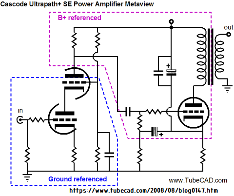
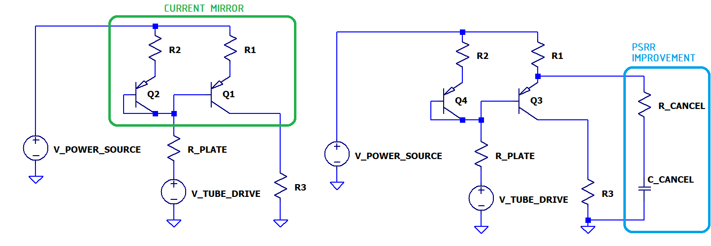
I want to be able to bias the input tube fairly high in current and still get a large output voltage swing. I couldn't make that happen with just a 300V B+ supply. But changing the tube's Cascode into a current mirror output, we can get some freedom in the input tube's bias points. In the current mirror block diagram below, R2 provides a fairly low impedance to the bottom tube's plate the same as the top tube does in the Cascode circuit above. Neither a tube cascode circuit nor the current mirror gives the bottom tube a "zero ohm" impedance to drive. However, both circuits will give the bottom tube a low enough impedance that the bandwidth goes up and the voltage swing on the plate is small compared to the bias voltage.
In the current mirror below, Q2 is wired as a diode so it can closely match the voltage curves of the Vbe junction of Q1. It is better to use the same transistor used for Q1 to make the "Q2 Diode" than it is to use a small signal diode or even just leaving the diode out. This Vbe matching reduces our distortion and the matching works in the real world, not just in SPICE. I have found that "diode" to "Vbe" matching that worked in SPICE did not always work in the real world particularly when you can't control both the manufacture and which FAB site they used for transistor and for the "diode".
In the current mirror, the ratio of R2/R1 is the current gain of the mirror.
Q1 will have a "relatively high" output impedance, but it could be made higher impedance and lower distortion by cascoding it.
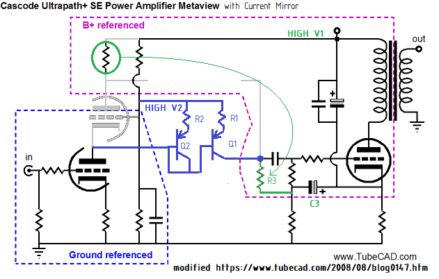
The topology above isn't the "Broken by the Cascode Guru Ultra-Path" from the TubeCad 0147 article that is shown below. The drive from the current mirror to the output tube going to "R3" is just skipping the coupling through the B+ to Cathode capacitor and is directly coupling to the "R3" in the cathode bias circuit.
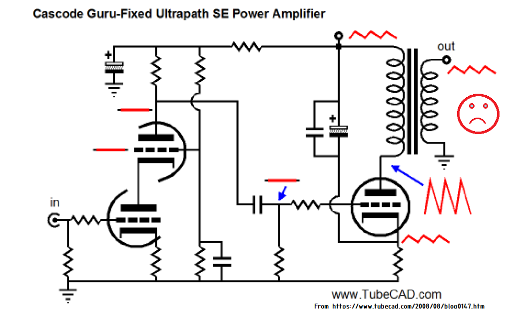
When we add a cascode to Q1 to make its output impedance very high, it allows the "Ultra-Path" magic to fully happen. A Cascode can also reduce the current mirror's output voltage distortion nearly 10:1.
Q3 is going to run hot. It will be hottest when 1/2 the available voltage is across Q3 and the other half is across R3. I'm going to parallel two "Q3" BJT parts to keep the temperature rise reasonable. When you parallel transistors, the emitter resistor in each of the paralleled transistor needs to drop 250mV at nominal current for good current sharing to occur.
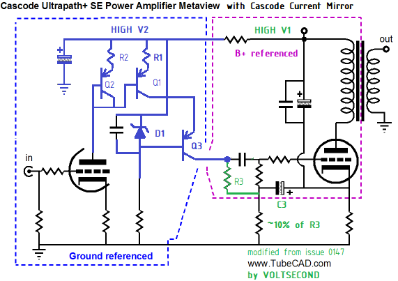
Uber-nerd note:
The 250mV for the emitter resistor comes from using ten times "nkT/Q". "nkT/Q" is from the I_base = Is * (E^(Vbe/(nkT/q) - 1) equation. The value "n" is normally close to 1, and we normally drop the "-1" in the equation in normal operation for it is small compared to the other numbers.
From the "Math" below, I found I wanted a "DC" current gain of about 1 in the mirror and wanted an "AC" gain of 2. To get a "DC" current gain of 1, on my first circuit I placed a blue LED (about 2.9V drop) in series with R1 to reduce the DC "current gain" while still keeping the "AC" signal gain at "2". There are more details about this in the "Version 1 of the Current Mirror (OK, but not great.)" section below.
Trying to be clever about this, I will also DC couple the bottom of R3 to the cathode of the driver tube to provide a little DC bias point stabilization. This will slightly reduce the sensitivity of the DC bias point to the gm of the first tube. Having run a few dozen variations of the circuit that aren't included here, the bias point needs just a little help to stay centered with part variations.
Instead of more design notes, I'll skip to the END and show the final circuit.
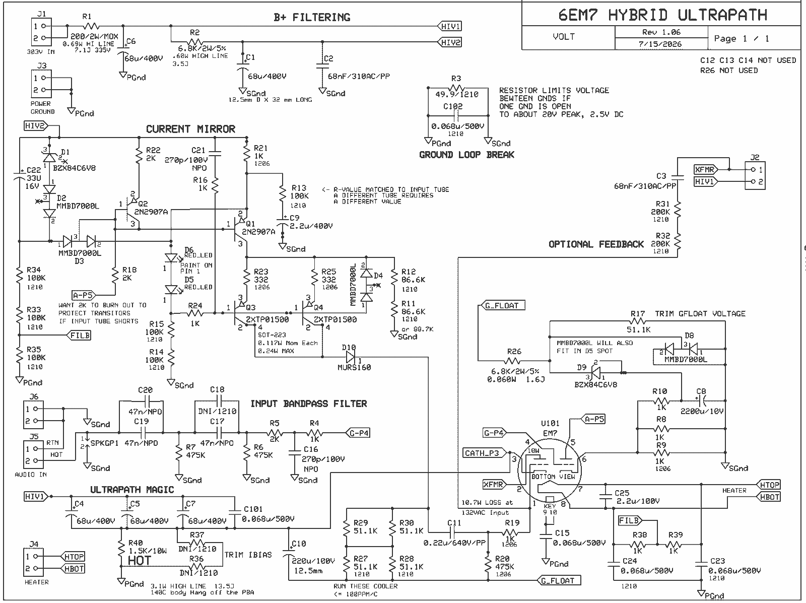
Below is what I am going to build. This is the "high power loss" driver version. LTSPICE indicated that the higher current draw version of the current mirror was about 10X lower distortion than the lower current LED Bias version. I'll throw away a few mA of driver current to get significantly lower distortion. There are parts on the board to add small amount of feedback from the plate to grid on the output tube. I'll try it both ways and use the way I like the best.
There are "trim resistors" on the board used to optimize the bias point. The tubes don't always behave like the SPICE model or Curves imply they will.
Near the end of this article, I'll give information on one possible 300V supply we could use.
A general rule of thumb is if you double the value of a resistor or capacitor and the inner loop or outer loop gain of the amplifier changes 2:1, buy a better part for that part. Thin film resistors are quieter and lower distortion than thick film resistors, but thin film often can't handle power surges. Use thin film for resistors that set gain. If you are stuck using thin film, don't run the resistors near rated power. I've found higher voltage film capacitors tend to be less microphonic than lower voltage parts of same value. NPO/COG ceramic capacitors tend to be sonically neutral where X7R/Z5U ceramic capacitors tend to be a sonic nightmare, but X7R can be worth while as power supply bypass.
|
Qty |
Name |
Order |
Part |
|
5 |
0.068u/500V |
399-13375-1-ND |
C101,C102,C15,C23,C24 |
|
1 |
0.22u/640V/PP |
495-2320-ND |
C11 |
|
1 |
2.2u/100V |
399-13375-1-ND |
C25 |
|
1 |
2.2u/400V |
1189-2724-ND |
C9 |
|
1 |
2200u/10V |
1189-2172-ND |
C8 |
|
1 |
220u/100V |
1189-2942-ND |
C10 |
|
2 |
270p/100V |
311-4395-1-ND |
C16,C21 |
|
1 |
33U |
478-12401-1-ND |
C22 |
|
3 |
47n/NPO |
445-CGA5H2C0G1H473J115AECT-ND |
C17,C19,C20 |
|
2 |
68nF/310AC/PP |
399-R523F268050P0K-ND |
C2,C3 |
|
5 |
68u/400V |
1189-400LXW68MEFR12.5X30-ND |
C1,C4,C5,C6,C7 |
|
1 |
DNI/1210 |
DNI |
C18 |
|
2 |
BZX84C6V8 |
353-BZX84C6V8HE3-TPCT-ND |
D1,D9 |
|
4 |
MMBD7000L |
MMBD7000LT1INCT-ND |
D2,D3,D4,D8 |
|
1 |
MURS160 |
MURS160-E3/5BTGICT-ND |
D10 |
|
2 |
RED_LED |
732-4989-1-ND_REd |
D5,D6 |
|
4 |
Hole_for_Wire |
None |
H1,H2,H3,H4 |
|
6 |
5mm_Two_Hole_300V |
732-10955-ND |
J1,J2,J3,J4,J5,J6 |
|
1 |
2N2907A |
MMBT2907A-TPMSCT-ND |
Q1,Q2 |
|
2 |
ZXTP01500 |
31-ZXTP01500BGQTCCT-ND |
Q3,Q4 |
|
1 |
1.5K/10W |
2485-40J1K5E-ND |
R40 |
|
6 |
100K |
541-100KAACT-ND |
R13,R14,R15,R33 |
|
9 |
1K |
RNCP1206FTD1K00CT-ND |
R10,R16,R19,R21, |
|
1 |
200/2W/MOX |
RSMF2JT200RCT-ND |
R1 |
|
2 |
200K |
541-200KAACT-ND |
R31,R32 |
|
3 |
2K |
RNCP1206FTD2K00CT-ND |
R18,R22,R5 |
|
2 |
332 |
RNCP1206FTD332RCT-ND |
R23,R25 |
|
3 |
475K |
541-475KFCT-ND |
R20,R6,R7 |
|
1 |
49.9/1210 |
RMCF1210FT49R9CT-ND |
R3 |
|
5 |
51.1K |
541-51.1KAACT-ND |
R17,R27,R28,R29,R30 |
|
2 |
6.8K/2W/5% |
13-RSF2WSJR-52-6K8CT-ND |
R2,R26 |
|
2 |
86.6K |
738-RMCF1210FT86K6CT-ND |
R11,R12 |
|
2 |
DNI/1210 |
NONE |
R36,R37 |
|
1 |
SPARK_GAP_PWB |
NONE |
SPKGP1 |
|
1 |
6EM7_Tube |
6EM7_EBAY |
U101A |
|
1 |
EM7 |
SK-B-VT8-PTS_TUBEDEPOT |
U101 |
You will also need an enclosure, power supply, hook up wire, an output transformer (Edcor 5Kohm SET), speaker posts, input RCA jacks, a volume control, hex posts, #4 screws, nuts and lock washers.
When choosing the SET output transformers, a transformer that is 1dB down at 40 Hz to 10kHz is usually 3dB down at 20Hz and possibly also 3dB down at 20kHz.
DNI means Do Not Install.
I am making an effort to only use Digikey Parts at this point. Not all parts I want are available at Digikey. Examples
1.4K 10W was not available. But it could be made with a 1.5K 10W with a 21K (20K 400V rated) across it.
51K 1W 25ppm/C 400V resistors were not available, but I could get 200V 100ppm/C 0.5W resistors and run them in a 2 watt array (half power for half the temperature rise).
While not a Digikey problem, these two issues have been plaguing me for years.
SMT (Surface Mount) resistors are seldom rated for more than 200V. You typically have to use two in series to get more than 200V across a single SMT resistor. I avoid the "special" ones that have a higher voltage rating. I got a really nasty shock at work when I specified the high voltage parts and the technician built my design with the cheaper low voltage parts. Missing the 200V by 10Vpk during occasional transients usually isn't a big deal. Missing it 2:1 steady state is begging to cash your insurance policies in.
SMT capacitors with a "20" in the part size are to be avoided. 1825, 2220 and larger caps are latent failures waiting to happen. If you can get them soldered without cracking them (I've seen cracks occur under the end caps where you can't see the crack), temperature cycling and or board flexing will crack them at some point. Oh, you're not going to abuse your design? What about your buddies that pick it up to look at it and let go of it 2" above the table when they set it down? Be proactive and just say no to big ceramics.
You will have to clean the board before using it. I would install all parts but the aluminum capacitors, clean the board, install the aluminums and clean the PBA one more time. I set the trace spacings up for a 300V B+ without conformal coat on the PBA.
When power is applied, the ultra-path ground and cathode of the output tube will surge up to nearly the full B+ voltage. The IPC voltage spacings apply under this condition as well as during normal operation.
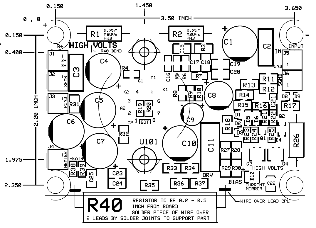
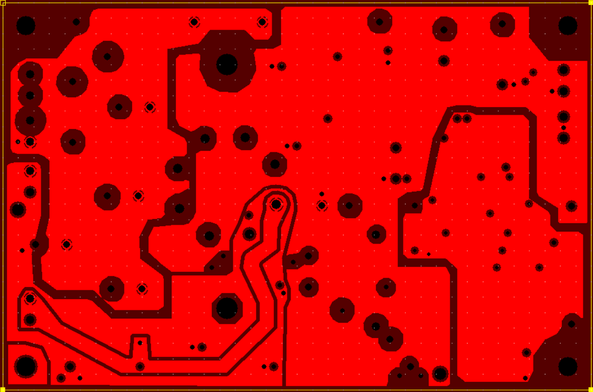
We should keep the edge of solder joints 0.1" or more from the edge of the board. A couple of Surface Mount parts may not be compliant with this in the view below, they should be fixed in the final version except for D9.
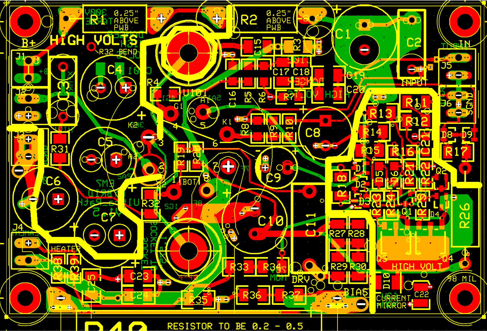
Top Left:
Cathode 2
Top Right: Signal Ground
Bot Right:
HIV2
Bot Left: PGND and Filament
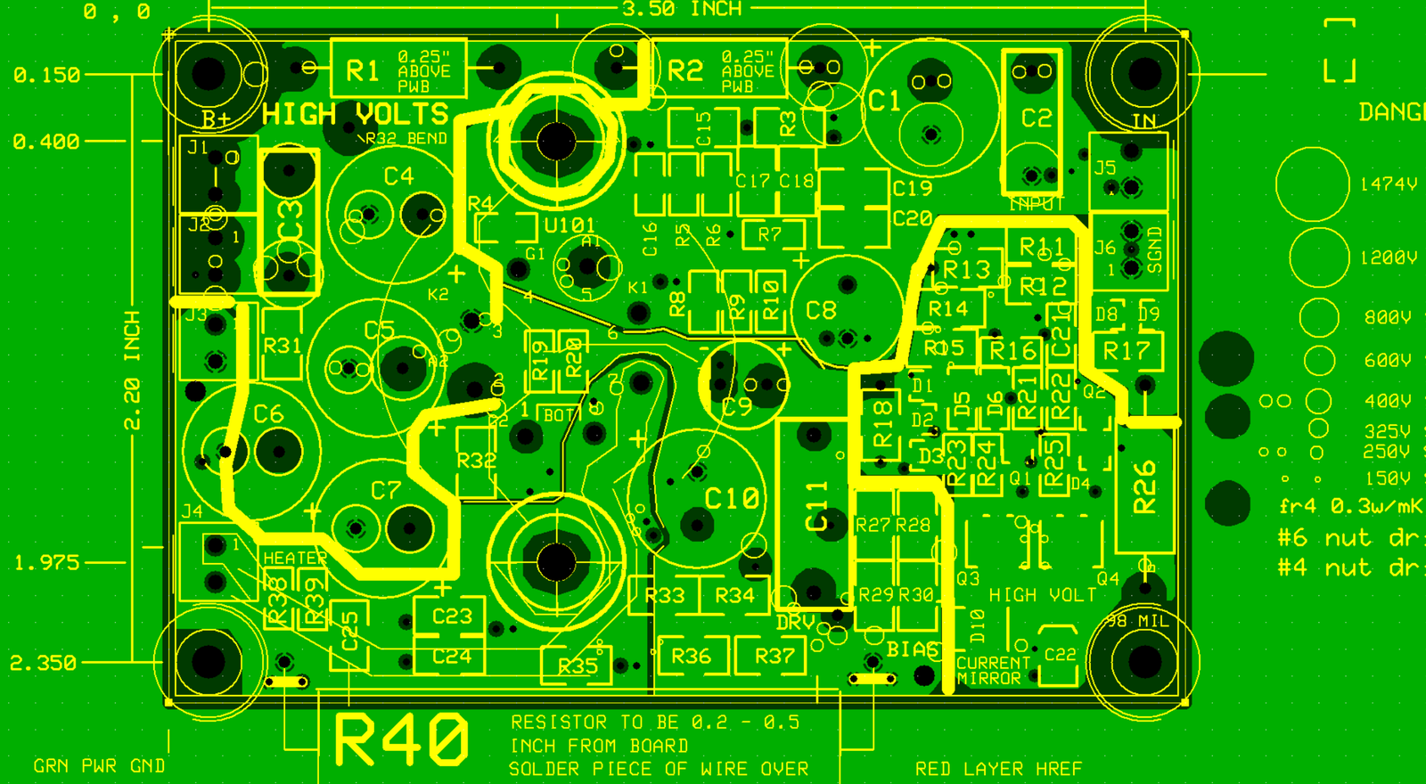
Top Left:
HIV1
Top Right: Signal Ground
Bot Right:
HREF
Bot Left: PGND
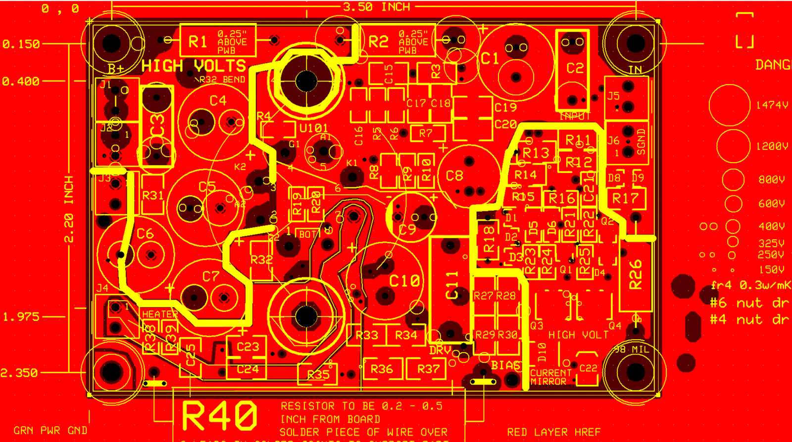
R40 hangs off the board. There is a hole called R40 bend just under R1 that can be used with the left edge of the PWB to set the second lead bend position "into" the PWB. This is not the bend next to the body of the part, but the downward bend into the PWB. There are extra vias next to the R40 solder joint to allow a lead from R1 to be soldered over the R40 lead to provide stress relief for the electrical R40 solder joint.
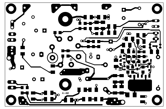
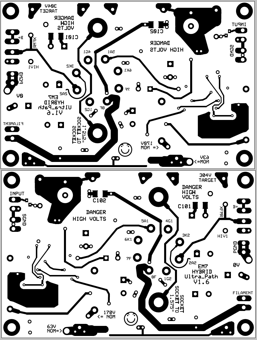
This is both X-ray view on top and normal viewing from the bottom. The tube socket installs from this side. Loosely install, 1/4 grunt tight ;-}, all mounting hardware that is going from both the tube socket to PWB and from chassis to the PWB before soldering in the tube socket. If you don't, you'll never fit it into the chassis with out ruining the PWB from re-soldering everything over and over to make it fit. If you make this mistake, save the PWB by cutting the leads off of the tube socket and then remove the leads one by one.
C101 and C102 are intended to be installed to "tune" the noise of the amp in the final installation. Start with C101 not installed and with C102 installed.
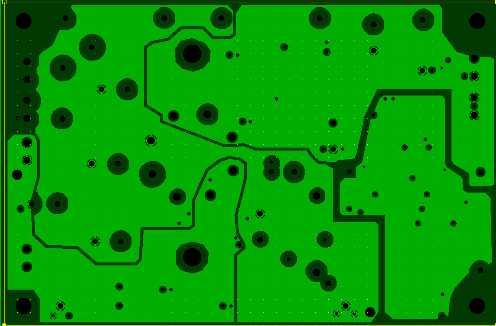
I attempted to round all of outward pointing high voltage corners on these planes.
The filament runs are run on top of each other to 1st order cancel the magnetic fields.
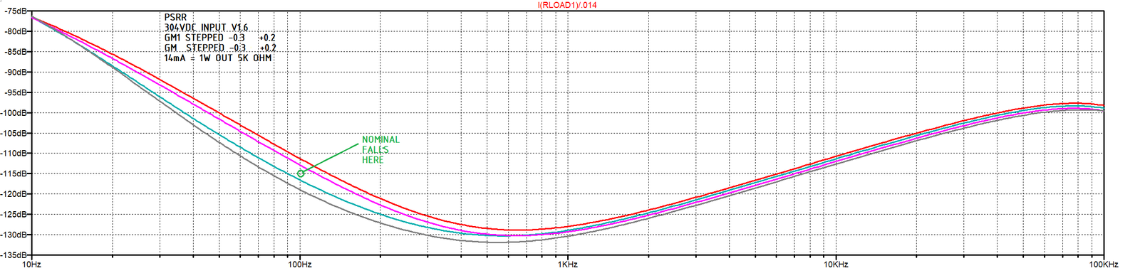
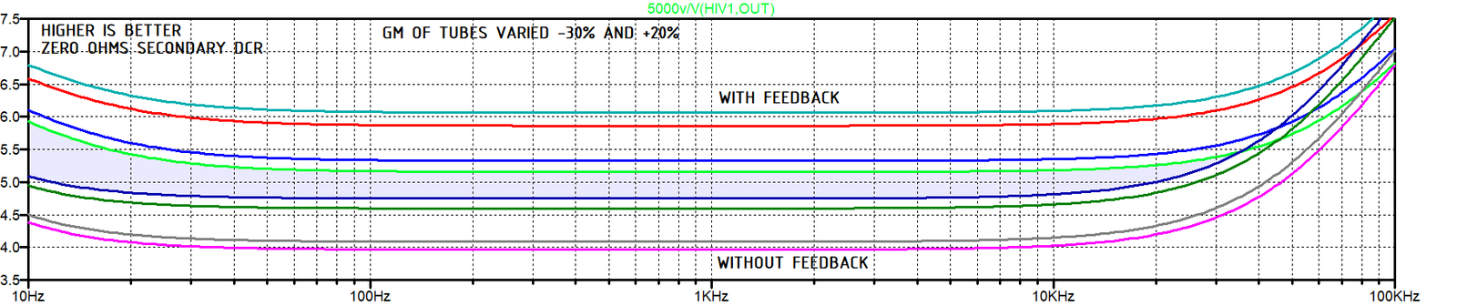
For PSRR, 1V was applied to B+ and the gm of the tubes was stepped between -30% (a tube with some wear left) and +20% (a high gain, new tube). From searching the net, -40% on gm is normally considered a worn out tube. I decided that plotting -30% was more important than plotting -40%.
This run is with a 68uF 400V capacitor in all locations. What I like about this is the high attenuation at 10Hz. Line voltage changes from the air conditioning kicking in and out shouldn't cause much of an audible impact.
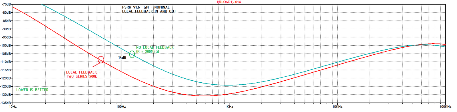
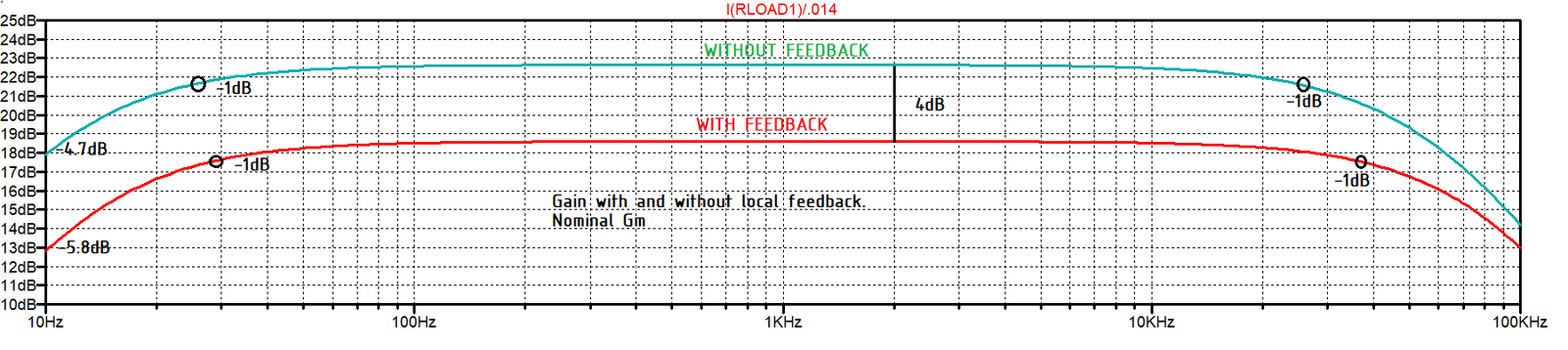
This run is with and without the local feedback on the output tube normalized to 1W output. I did not check to see if I could "retune" other parts to improve the performance without the local feedback.
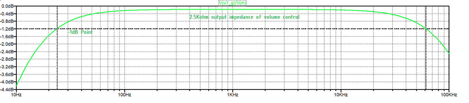
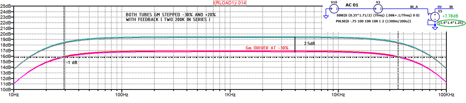
The frequency response curves are made with the Band Pass filter in place with a 2.5K output impedance from a volume control. The low frequencies are rolled off to prevent wasting current in the output transformer at frequencies it won't produce. The high frequencies are rolled off to prevent RF and ultrasonics from impacting the driver tube. The mid-band amplitude is down 0.17dB because of the two 475K resistors to ground working against the volume control's impedance.
Output response with Gm at -30% and +20%. The change in gain of the amplifier with changes in gain of the driver tube is a good reason to match the input tubes and/or to have a balance knob on the volume control. However, I really doubt anyone would be using an over performing new tube in one channel with a worn, but usable, old tube in the other channel.
For the AC "gain" measurements, the input voltage was 2.45V, not 1V.
This is the predicted frequency response with and without local feedback on the output tube.
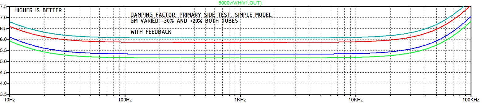
With local feedback on the output tube, the damping factor (without secondary DCR) looks like this:
Local Feedback on the primary side improves the damping factor by a factor of 1.28:1. With even more feedback, higher available gate drive current swing and part re-tuning we can improve the damping factor further, but we risk breaking other things. Like many things, a little feedback can be good and too much feedback can be a problem.
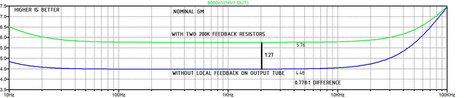
For the fun of it, let's sweep the Gm and Vary the Feedback at the same time. Feedback raises the damping factor in all configurations.
With 1W into 5K (100Vpk), 304V input, 40.85mA Bias, 8.94W Plate Loss,
with feedback the total distortion was 5.48%,
without feedback the total distortion was 7.46%.
The results for the first seven harmonics are shown below.
|
Harmonic |
Frequency |
dB With |
dB
Without |
dB
Feedback |
|
1 |
1.000e+02 |
0.0 |
0.0 |
0.0 |
|
2 |
2.000e+02 |
-25.2 |
-22.6 |
2.7 |
|
3 |
3.000e+02 |
-57.7 |
-46.9 |
10.8 |
|
4 |
4.000e+02 |
-67.5 |
-61.0 |
6.5 |
|
5 |
5.000e+02 |
-91.8 |
-83.0 |
8.8 |
|
6 |
6.000e+02 |
-92.9 |
-90.3 |
2.6 |
|
7 |
7.000e+02 |
-98.3 |
-92.2 |
6.1 |
Feedback dropped the 2nd harmonic by 2.7dB, but more importantly, it dropped the 3rd harmonic by 10.8dB.
A SPICE reminder: When using the .FOUR command to do a Fourier sweep, make sure that "data compression" is turned off and remember that the reported output voltage is in peak volts, not RMS volts.
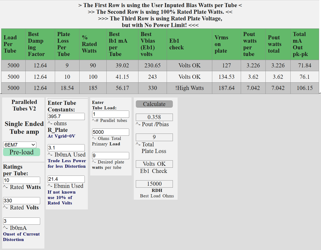
We will plan on controlling B+ to 10% so we can push the 10W rating of the tube to 9W.
Normally we would plan on a 5K plate load feeding 8 ohms out. The speaker load of 8 ohms isn't a real 8 ohms. It will have impedance dips in it below 6 ohms, but designing for a dip to 6 ohms is all I want to adjust for at this point.
Going to the Parallel Tube Calculator and setting the number of tubes to "1" we get:
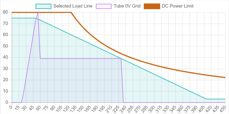
5K Load Line will look like this:
Now let us repeat this for a Plate Load of 6 ohm/8 ohm * 5K ohm = 3750 ohms
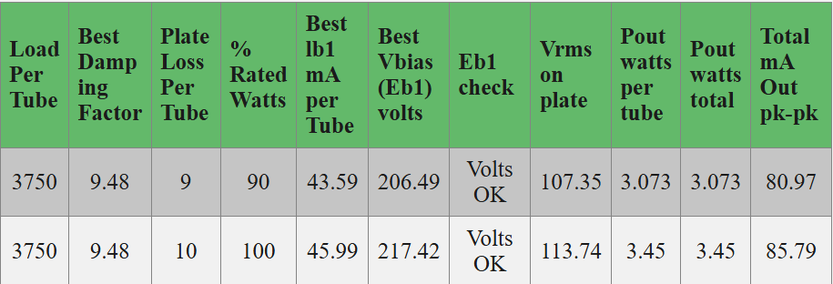
The 5K Bias Point wants a 230V Plate to cathode voltage and 39mA. The 3750 ohm Bias point wants 206V and 43.6mA. We can compromise between the two and bias for 218V and 41.3mA. Going to the tube's curves we find this will require -36V grid to cathode.
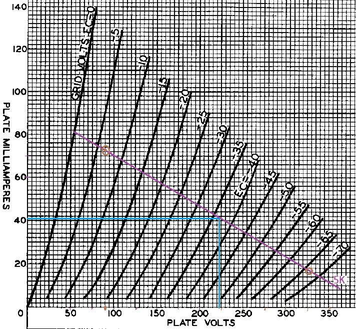
No, the bias point math is not wrong. The output power in SPICE is low because the bias point is calculated for the linearized plate's response swinging the grid from 0V to the bias point. Looking at a +30V swing, in this 5K case, a ~155V swing occurs on the plate (2.402W into 5K). If we go from the bias point to bias point -30V (-67V), we get a ~107V plate swing (1.145W). The average of the two powers is 1.65W. This becomes a 6 peak difference, 3.2 dB peak to average difference in the powers. With the bias point math we'll see 3.1W out, but we should expect 1.44:1 less power, or 2.07W out, if measured with more complete tube model.
This falls under "The devil is in the details" OR "Statistics don't lie, statisticians do" or what ever euphemism you would like to use instead. Things like this used to drive me bats, now, not so much. If Ib0 in the calculator is set higher, this issue is reduced, but the maximum output power (distorted) also is reduced.
From the 6EM7's data sheet, the Anode (Plate) to Grid capacitance is 10pF, the Grid to Cathode capacitance is 7pF and the unloaded amplification factor is 5.4. With a 5K load, the loaded amplification factor drops the effective Av to be 5.4 * 5K/(5K+ 0.75K Rplate output tube) = 4.695.
The effective input capacitance at the grid is Cin = Cag * (1 + Av) + Cgc = 10pF * (1+4.695) + 7pF = 64pF.
I'd like the output tube (not counting the transformer) to be 1dB down at 20kHz. To get 1dB down at a frequency, you need to set the 3dB down point to be at twice that frequency.
For 3dB down at 40kHz, we want to drive the grid with less than 1/(40kHz * 2 * PI * 64pF) = 62K. I'll use 51.1K
Repeating these calculations for the input tube that will be used as the bottom tube of a Cascode Gain Stage.
Cag = 4.8pF
Cgc = 2.2pF
Rplate = 40kohm
Rload = 4kohm (estimated)
Av = 4K/(4K + 40K) = 0.091 (Av being near zero is normal for the bottom tube of a Cascode)
Ctotal = 4.8pF * (1+0.091) + 2.2pF = 7.44pF
Rmax = 1/(40kHz * 2 * PI * 7.44pF) = 535K
Rmax is the total resistance in series with the gate (Signal source, Volume Control, Series resistors). This is not the resistance to signal ground.
If we want to roll off the input tube in the 100kHz range, we will be better off using a series RC filter between the input jack and the gate than the input capacitance of the tube.
From a driver, I normally like to be able to swing 1.5 to 2X the minimum needed to drive the next stage. I want to "provision" for local feedback on the output tube (a cap coupled resistor from Plate to grid) to lower the amp's output impedance slightly. 6dB feedback is the most I would want to use. This local feedback effectively doubles the current swing needed by the driver (or doubles the DC bias across the 51K resistor). So we have to plan on 3–4 times 36Vpk on the 51K (108 to 144V or 2.1mA to 2.82mA steady state.) The 1.5X minimum margin will pay for the 475K resistor directly on the output tube's grid.
With 1Vpk input we want to deliver the 1.5 to 2X output drive level. This is 2.8mA drive on the high current side.
2.8mApk / 1Vpk input / 2:1 for mirror gain = 1.4mA/V = 1400 umhos = (1/714 ohms)
On the low current side 2.1mA, or 1/952 ohms, will be needed. Our input (driver) tube is specified at 1600 umhos (625 ohm). I'd like to linearize this gain with an un-bypassed cathode resistor to reduce distortion. If we add 333 ohms in the cathode of the driver we get 958 ohms which is close enough to the range of what we calculated we need.
I drove the filament bias circuit with an estimated transformer line to filament parasitic of 2nF. This is from the 120V to the filament. The model predicts that at 100 Hz the noise is 95dB down when compared to 1W output. At 1kHz is it 108dB down. With the planned bypass, we don't have worry about filament noise through the current mirror. I'm not showing the plot for this. I was boring even for me.
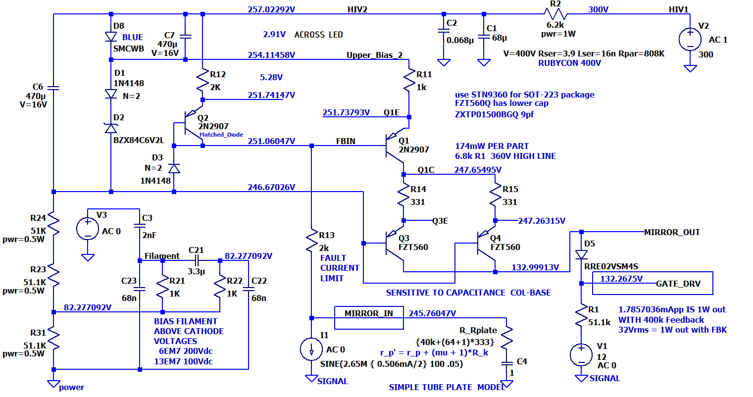
Below is the first current mirror version I planned for use on the Printed Wiring Board. The bias point voltages are shown.
D8 is a Blue LED that removes 2.9V from the voltage that normally would appear across R11. This lowers the Mirror_Out current at DC without wasting extra HV current. R12/R11 will set the AC current gain of the circuit. And we can get the gain we want.
The Base of Q1 (FBIN) is clamped to a zener voltage reference by D3 to protect the transistors during over drive events. I do this because you never want to reverse bias the base-emitter of a transistor by more than about 5V. If you do, you'll both make the part noisier and lower it's current gain. SPICE doesn't cover this issue in the standard BJT model.
The same voltage reference used to limit the drive into the transistors becomes the voltage reference for the output Cascode transistors. This voltage reference is bypasses with a fairly large capacitor to limit zener noise and to reject voltage ripple from the B+ input and the Bias Drive for the filaments. The LED is bypassed with a capacitor to reduce distortion.
At this point, this circuit is "NOT YET A PROPER ULTRA-PATH". R1 must be capacitor coupled to HiV1 for this to be an Ultra-Path
32V
peak on GATE_DRV is equivalent to 1W into a 5kohm on the output tube.
This voltage is with an assumed 400K local feedback resistor plate to
grid on the output tube.
At that 32V output, this circuit
generates 0.012% 2nd harmonic and 0.021/% 3rd harmonic distortion. At
half the drive level, which occurs when the local feedback resistor
is removed, the distortion is about 2.8X lower.
Looking at the Power Supply Rejection Ratio, the mirror (Blue) was expected to do fairly well. The plate resistance of the driver tube dominates how much voltage ripple makes it to the Gate Drive from B+ ripple.
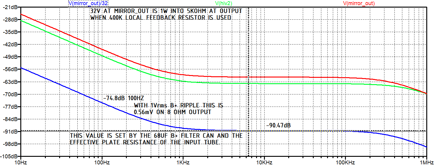
We missed the interaction between the output impedance of the Cascode and the 51K gate resistor.
The output impedance of the current mirror is 13 megohm at 1kHz and 1 megohm at 20kHz (8pF). This is reasonably good for an output impedance from a non-Hawksford cascode that is using two transistors in parallel for the output. At 1kHz, a 13 meg output from the current mirror feeding 51K on the gate should give 48dB attenuation to any cathode voltage ripple. With 32V needed on the gate to make 1W out, this 48 dB drops down to 78dB of rejection at 1kHz with respect to 1V of ripple on the cathode. While only 12dB worse than the plot (3 plots) above at 1kHz, the rejection becomes significantly worse (less) as the frequency increases. At 20kHz it drops to be 56dB, We'll look at this in more detail later.
The PSRR is limited by the ripple voltage that is on HiV2 placing a ripple voltage across the effective Rplate of the driver tube (40K + (63+1)*333ohm). With an effective plate resistance of 61.6Kohm, 3.55mV of ripple (100Hz from green plot above at 100 Hz) makes 57nA of current noise into the mirror. The Mirror multiples this by 2 and into 51K this becomes 5.88mV which is 75dB down with respect to 32V. This reasonably matches the blue line in the plot above.
With an infinite plate resistance on the driver tube, the PSRR is 132dB down at 1kHz instead of around 90dB down. This was the clue that the tube is part of the less than perfect PSRR performance issue. When the tube makes a drive voltage, it feeds it through its R_Plate into the current mirror and the current mirror then drives R3, the output. Now if the power supply has noise voltage on it, it also drives a current through R_PLATE which is amplified by the current mirror and fed into R3.
If we place a capacitor to signal ground with a series resistor to Q1E (the 1K "gain" resistor) we should be able to inject a cancellation current into the current mirror to improve the PSRR. Rplate increases with tube age, so we'll want to set the cancellation resistance value 10 to 20% higher than "optimum" so the amps sounds good with both an old tube and with a new tube. First order, this resistor value is equal to Rplate Effective / Current Mirror Gain. The capacitor to signal ground should be picked for long life, reasonable leakage current and an RC corner between 1 Hz and 10Hz The upper limit of 10Hz is picked so that at 20Hz, the RC is within 1dB of its final performance boost. 1Hz is picked because we don't want the circuit to take too long to settle into it's DC bias point. I found 2.2uF 400V electrolytics with good lead spacings readily available. At my preferred value of 1uF, the lead spacing was too close together for my comfort and I didn't have room to use a 1uF film capacitor.
First order, R_Cancel = R_plate * R1 / R2
The downside of the cancellation circuit is that R_Plate is variable. It increases as the tube ages, and it changes with the tube's bias point as seen in the curves below, and it changes with the tube. So what do we do? We set the R_Cancel on the high side and live with non-perfect cancellation for the cancellation still helps even if the cancellation isn't perfect. In the Mirror Circuit comparisons, I'm using a nominal value for Rplate. For the final version, I'll tune the circuit with an actual tube in place.
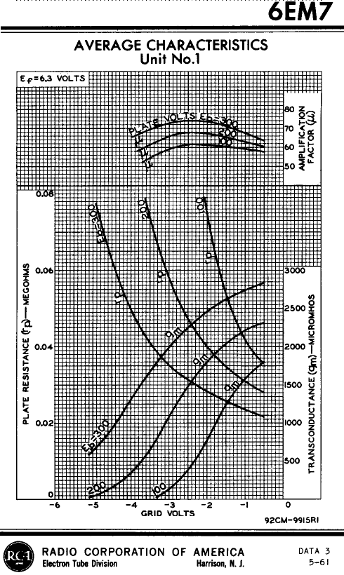
From the 6EM7 Input Tube Curves, we see that Rp varies greatly; this is from the variation in "gm". The tube amplification factor, "mu", doesn't vary much.
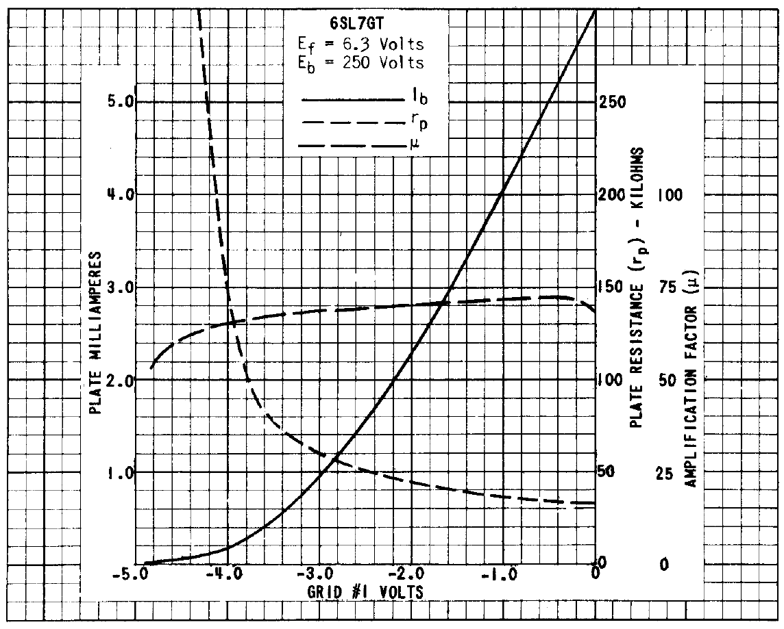
6SL7 Curves also vary. (The flattest curve one is the "u" curve.)
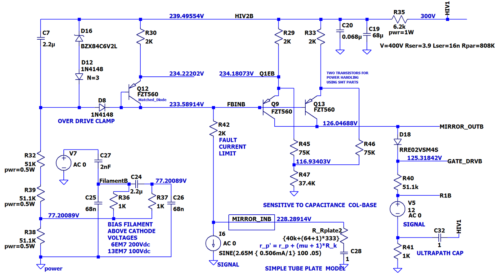
This is the current mirror with R45-R47 providing both plate current compensation and the DC Bias Correction. A 2.2uF capacitor across R47 (37.4K) provides 3dB improvement at 10Hz but provides NO IMPROVEMENT over 50 Hz. With no improvement over 50Hz, the part isn't worth adding. This circuit can also be built with the BLUE LED DC Bias Correction if you want to save a little B+ power.
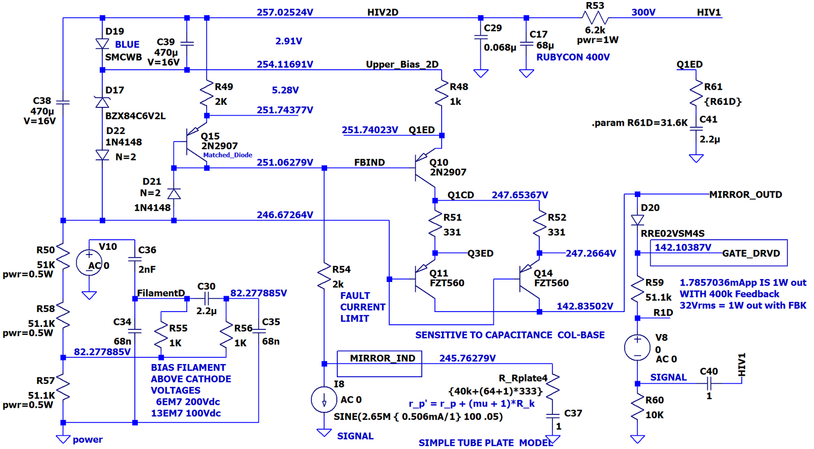
The BLUE LED providing the DC offset reduces the current draw from the high voltage B+, but it increases the amount of B+ noised that makes it to the output at less than 10 Hz. The LED is bypassed to reduce high order distortion products. These were fairly low level harmonics, but the capacitor fit on the first board layout pass, so I used it so I could compare with and without at some point. The final design didn't use the BLUE LED for DC current reduction.
In this simpler Cascode, the DC bias point correction occurs by using R44. R44 draws output current away "AFTER" the current mirror. This biases Q5 further into Class A which reduces the distortion from the current mirror. This distortion reduction costs us higher power loss. However, I'll throw away 0.8W of power in the driver to reduce distortion. R44 also acts as Plate Resistor Feed Forward (PSRR correction), so R62 ends up as at higher value resistor.
Q6 and Q7 will need a protection diode (1N4148, not shown) across them to prevent Vbe avalanche with a cold driver tube.
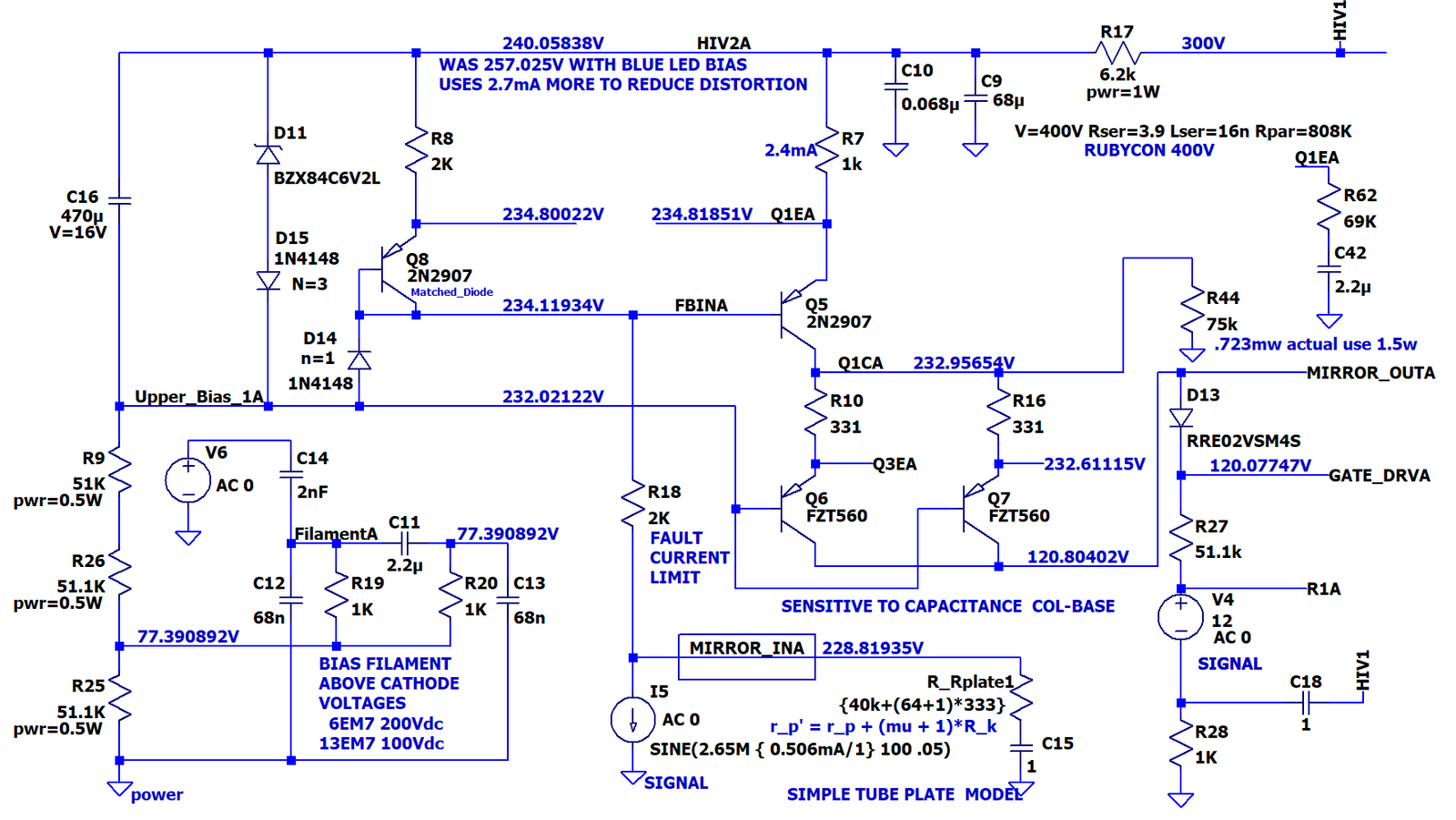
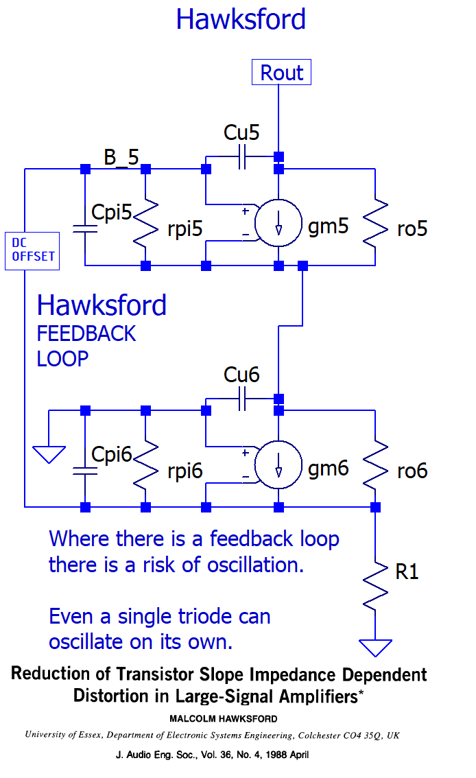
The above Cascodes do not correct for the ripple induced from the output impedance issue of the Cascode. To do this, we need to switch to that "Twitchy, Hawksford Cascode." The Hawksford cascode increases the output impedance of normal cascode often by 40dB. It also can reduce the current distortion coming out of the Cascode. Why is it "Twitchy"? If the signal routing isn't done right and the "Grid Stop" resistors feeding the Hawksford cascode aren't correctly picked, the Hawksford Cascode will ring and/or oscillate and create more distortion than if we stuck with a simple Cascode. A simple cascode can oscillate, but a simple grid stop resistor is usually all it needs.
Notes:
1. With really long wiring and a horrid layout, a single transistor can be made to oscillate.
2. I've seen a guy do the "equivalent" of twisting the base of the current mirror wires with the B+ transformer leads and then wonder why the circuit was noisy.
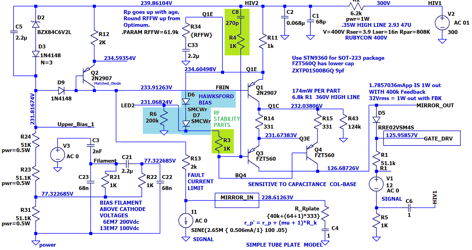
The Hawksford Cascode version with Plate Resistor Feed Forward (R34) and "lower distortion" DC bias correction (R43) is shown below. The Q3, Q4 cold tube protection diode is not installed at this point.
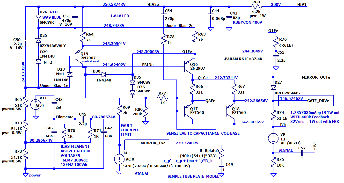
Below is the Hawksford Cascode with RED LED DC Bias Correction. At 1kHz AC this is very similar to the resistive bias correction version except for the tuning values. At 10Hz this design is worse than the Hawksford with Resistive DC Bias Correction. At low frequencies, it behaves like the standard Cascode with Blue LED DC Bias Correction.
I won't be providing AC plots for this because the output distortion is not good for this design and at some bias points it can have problems driving the RC Plate resistance RC network.
D26 had to be changed from a Blue LED to a RED LED to get the Mirror_Out to bias up correctly.
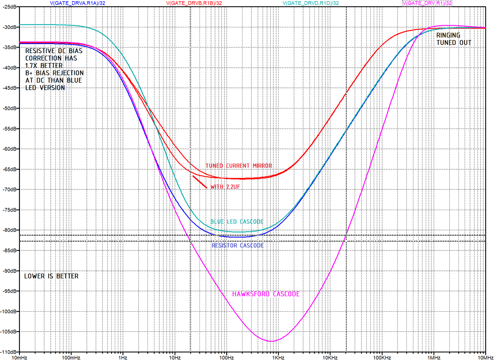
These plots are with respect to 1W output with the 6dB local feedback on the output tube. With the feedback removed, the PSRR gets 6 dB worse (noisier, not quieter).
At 1kHz I could live with the normal Cascode. The power supply "should be" quieter at 20kHz than at 1kHz, but I'm not sure if I'm willing to risk the normal Cascode's PSRR at 20kHz. When you build things, the performance doesn't always match the SPICE analysis because of sneak paths from wire to wire coupling, part to part coupling and less than perfect parts and models.
I'm definitely willing to trade a little more power loss to use the resistive DC bias point correction of the voltage on the 51K gate resistor over the Blue LED bias point compensation.
The output impedances of the mirror circuits are as shown below. The Hawksford version performs the best. The Simple Mirror version performs the worst. However, the Hawksford configuration is sensitive to layout.
While I've made the Hawksford work in the MHz region with "tuned up" PWBs, I find it easiest to stabilize and be forgiving by turning it back into a standard Cascode somewhere above 100kHz.
Higher is better in the curve below.
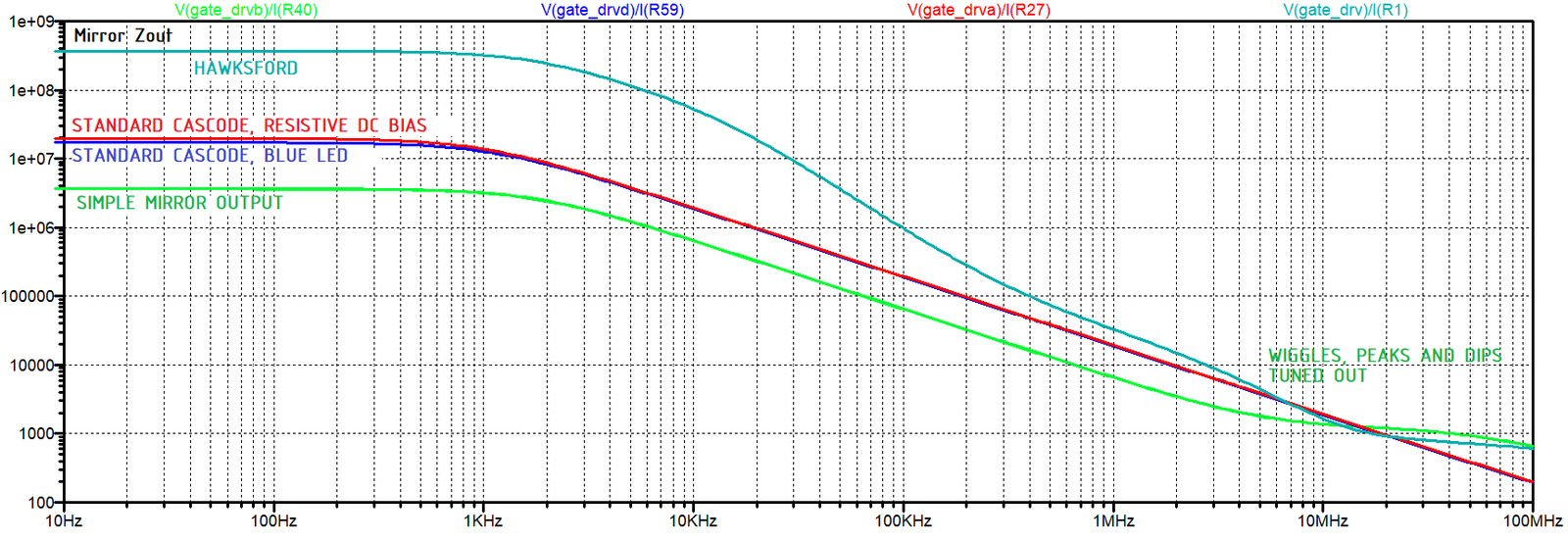
This is before any tube distortion is added in. We want the tubes to be the dominant source of any distortion, not the supporting solid state parts.
The Hawksford with Resistive DC Bias Correction performs the best. The Hawksford with Blue LED DC Bias Correction had significantly higher distortion than the Hawksford with Resistive DC Bias Correction version. This is because the bias current for the two Hawksford LEDs steals current from the current mirror's output transistor reducing how far into Class A the parts are biased.
The Simple Cascode's performance versions aren't simple to compare. In the simple Cascode, the Blue LED DC Bias Correction version has lower THD, the resistive DC Bias Correction has a much lower 3rd Harmonic. The higher THD is from the higher 2nd harmonic. I prefer the design with higher 2nd harmonic distortion that has the lower 3rd harmonic.
|
|
Simple
Mirror |
Simple
Cascode |
Simple
Cascode |
Hawksford
Cascode |
Hawksford
Cascode |
|
|
V Fundamental 51K ohm |
47.39 |
48.70 |
48.11 |
49.20 |
49.08 |
Volts |
|
Normalized 2nd Harmonic |
1.52E-03 |
1.12E-04 |
7.80E-04 |
1.32E-04 |
1.16E-03 |
Relative |
|
Normalized 3rd Harmonic |
4.92E-04 |
2.71E-04 |
9.81E-05 |
2.34E-05 |
2.03E-04 |
Relative |
|
THD |
0.1597% |
0.0293% |
0.0785% |
0.0134% |
0.1180% |
Percent |
|
|
|
|
|
|
|
|
|
Normalized 2nd Harmonic |
-56.4 |
-79.0 |
-62.2 |
-77.6 |
-58.7 |
dB |
|
Normalized 3rd Harmonic |
-66.2 |
-71.3 |
-80.2 |
-92.6 |
-73.8 |
dB |
|
THD |
-55.9 |
-70.6 |
-62.1 |
-77.5 |
-58.6 |
dB |
|
|
|
|
|
|
|
|
There Ain't No Such Thing As A Free Lunch (or Free Variable)
The PSRR feedforward resistor and the Rplate RC cancellation additions requires a couple of changes to add reverse polarity protection for the Vbe of the transistors. If the transistor's Vbe is avalanched, it will degrade both the Hfe and the noise characteristics of the BJT.
Using the Hawksford Cascode as the example, when the tube is pulled or the filament is cold, the Cascode output transistor's Vbe is avalanched by the DC bias adjustment resistor to ground. During power-up, the Current Mirror transistor is reverse biased by the RC plate cancellation parts to ground. The power-up issue does not always occur, but we should plan for it in case we make changes to the design. Both of these issues can be fixed with a simple small signal diode across the base to emitter on the transistor.
We have to add a diode to protect the output transistors. We can shift the existing diodes around to protect the current mirror transistor if we change the 6.2V zener into a 6.8V zener. From the curves from the Motorola 1N4733 and Microsemi 1N5525 datasheets tables are shown below, the 6.8V will be a good actor in the circuit. I'd be a little concerned with noise risks if we switched to a 8.2V Zener.
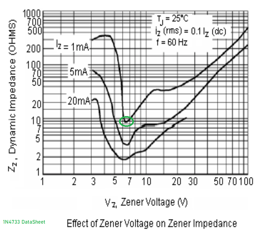
6.2V
zeners have near the optimum trades in performance as seen in this
capture of a Microsemi datasheet.
Zeners are noisier at
very low current than at moderate currents. Unfortunately, I can't
find the zener noise vs current curve I once saw.
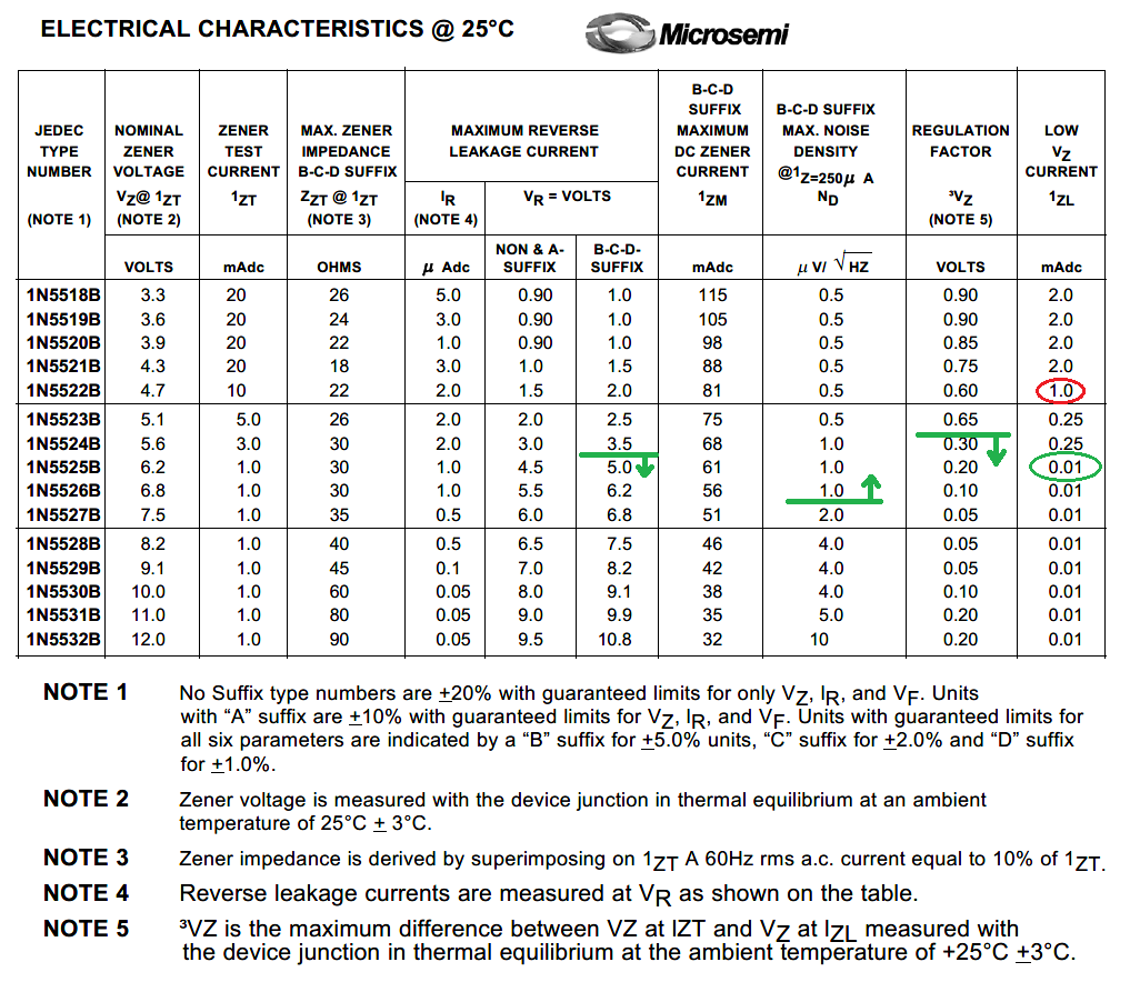
The protection changes are shown below.
D2 changes from 6.2V to 6.8V
D3 goes from 3 diodes to 2 diodes in series
D24 added to protect Q1 (this diode already in the MMBD7000L dual diodes used in the PWA (Printed Wiring Assembly)
D23 added to protect Q3 and Q4. Two diodes are used in series because they were already available in the MMBD7000L and theoretically, it should work better because of the lower capacitance.
With these changes, D9 clamps the input at about the same operating point as when Q3/Q4 go into saturation. This minimizes the interaction with normal operation.
The new diodes did not impact the distortion performance or Zout or PSRR.
Below I'm coupling the output of the current mirror into the cathode of the driver tube to help stabilize the bias point for changes in the gm of the driver tube. I'll be happy with even a small improvement in the bias point stability.
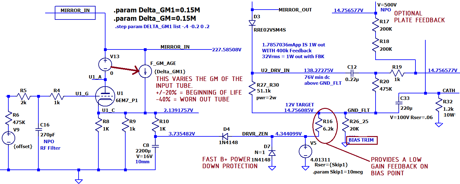
With the bias loop disabled (series resistance of V5 = 0.1 ohm) and r26_25=20k
.step
delta_gm1=-0.4
.step delta_gm1=-0.2
.step
delta_gm1=0
.step delta_gm1=0.2
Without the small amount of DC bias point feedback we get a 2:1 swing in bias point for a 2:1 swing in the tube's gm.
step AVG(V(U2_DRV_IN,GND_FLT))
1 88.1507511143
2 108.815281869
3 123.507227898
4 134.534071923
With the loop enabled (R series V5 = 10 megohm)
step AVG(V(U2_DRV_IN,GND_FLT))
1 75.5344648365
2 107.625675202
3 132.606625557
4 152.627529145
With the feedback we get a 1.52:1 swing in the bias point with the feedback for a 2:1 change in the driver tube's gm. This is not spectacular, but I just wanted a little improvement and 25% improvement is enough to help.
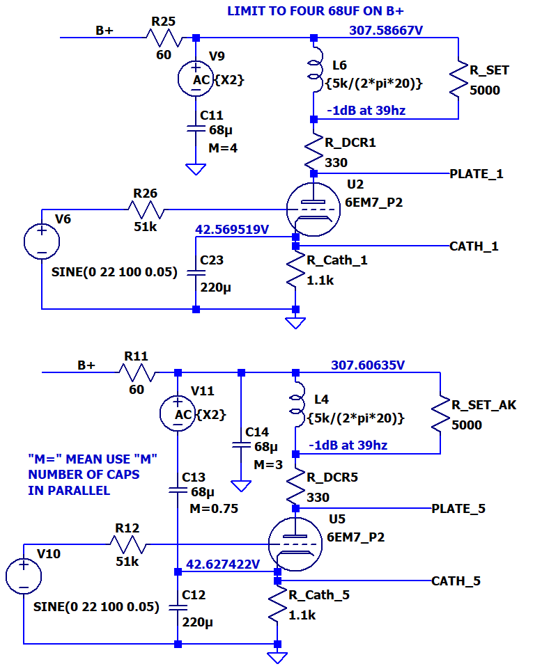
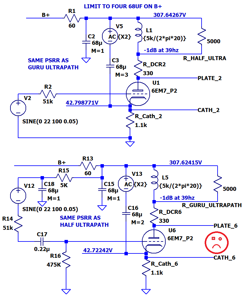
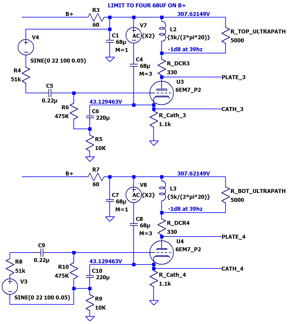
Let's compare the "ideal" output stage B+ capacitor possibilities. I will limit the number of B+ capacitor to be 4 total. The output tube's cathode capacitor doesn't count towards the 4. The circuits have ESR in the capacitors, but do not have all the other coupling paths for power supply noise that exists mostly in the driver tube part of the circuit.
First there is the standard SET arrangement and the semi-optimized "Aikido" version below it. I swept the value of C13 to get nearly the best performance possible. If C13 is slightly smaller, there was a resonant notch near 20Hz of better performance, I didn't use that value cap because I was figuring that Murphy would impose TANSTAAFL Karma on me later and the resonance of good PSRR would become a resonance of something else not being good.
Next is the unhappy faced "Cascode Guru" amp and a Half Ultra-Path where moving the B+ capacitor from signal ground to the cathode was the only Ultra-Path change made, the grid to cathode coupling change was skipped. In all cases, these two performed equally as BAD. There are many advanced topologies in engineering where if you don't want to mess things up, you can't go half way when making the change, it is all in or nothing.
Now there is the Ultra-Path versions. One couples the bulk of the grid drive to B+ (Top coupled) and the other couples the grid drive to the cathode of the output tube (Bot coupled). The Hybrid Current Mirror falls under the Bot_Ultra-Path group of performance.
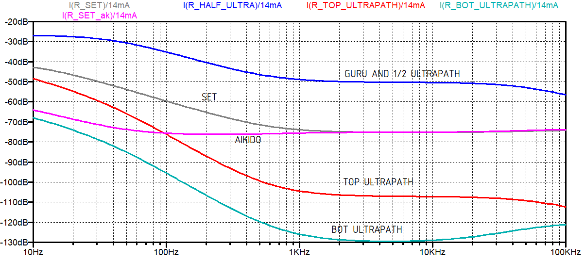
The Power Supply Rejection Ratio (PSRR) is how well the amplifier rejects power supply ripple.
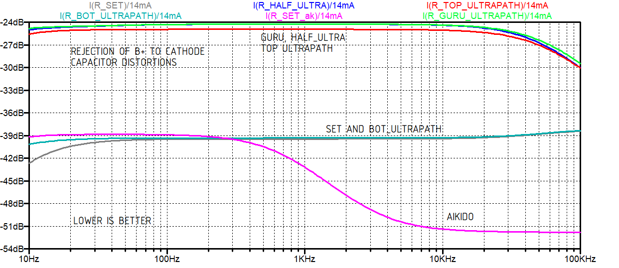
So you can say you don't care about a little hum. I can understand that. But the power supply often has noise at every harmonic of the line frequency and the power supply ripple will modulate the tube's output signal generating Inter-mod distortion. In the plot below I normalized the outputs to 14mA RMS into 5K ohm (1W).
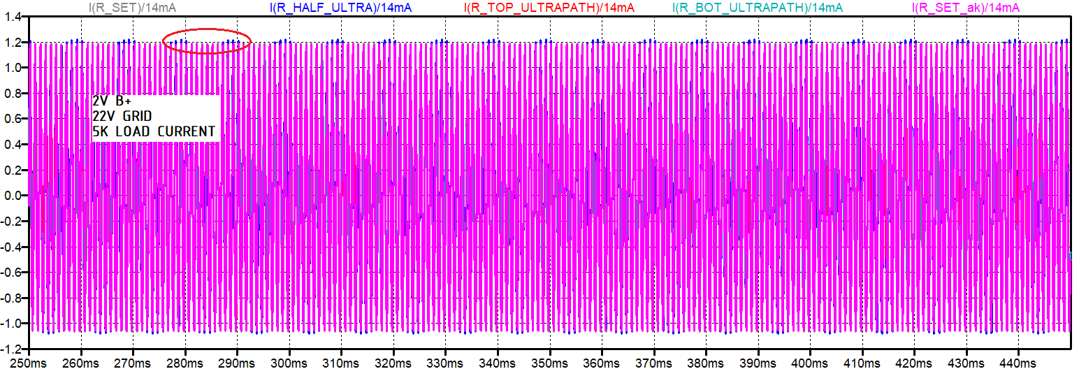
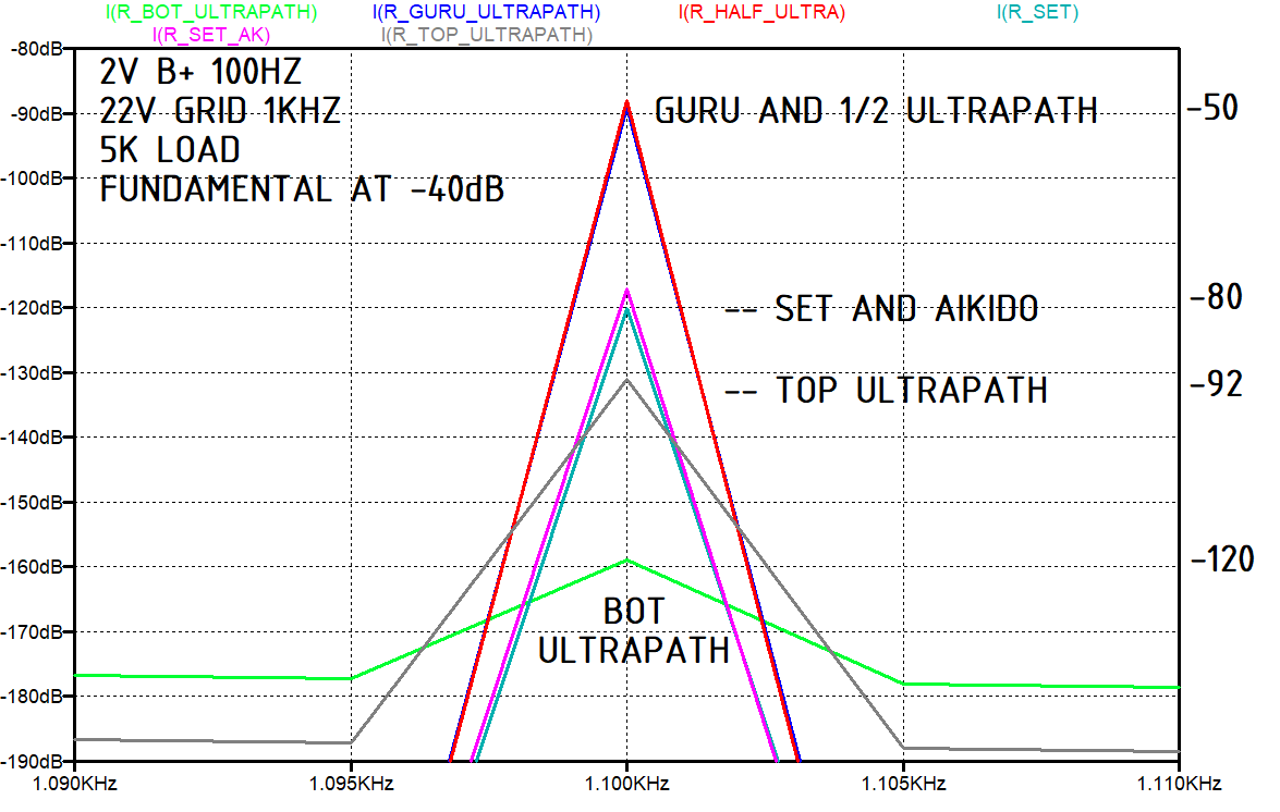
Below is what happens when we inject 2V of ripple into B+ (before the 60 ohm resistor) and 22V on the grid (about 1W out) and look at what happens to the current in the 5K ohm plate load. We can see that there is Amplitude Modulation (AM) of the output signal
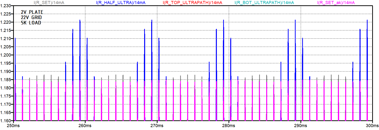
Let's zoom in. The Guru and Half Ultra-Path performance is not very good. I don't know exactly when it becomes audible, but I would like my amp not to have AM on the output.
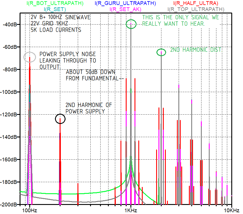
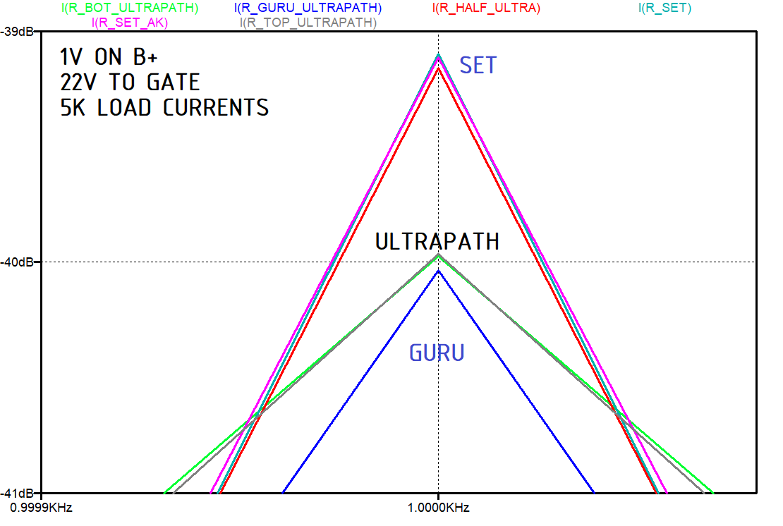
I can hear someone already saying "So What!". . .Well, mole hill, meet the mountains. . .Below is what we are sending to the speaker with the 1 kHz fundamental at about 1W output. The only signal I'd like to be sending to the speaker is the 1 kHz fundamental and possibly a little 2nd Harmonic. The rest is unwanted.
This is a zoom in of the fundamental, except it is at 1V instead of 2V on B+. The 1 to 2V ripple difference doesn't change this plot. The fundamentals are slightly different by about 1dB or 12%. This is because the Ultra-Path and Guru circuits have a 475K resistor grid to local ground and the others do not. What we want to see here is that the 1kHz signals are about the same amplitude and they are.
Below is what is going on at the fundamental frequency plus 100Hz. The inter-mods of the Guru version are only 50dB down from the main signal. The Bottom Referenced Ultra-Path is performing great. The Top referenced Ultra-Path is acceptable. The Hybrid Mirror we are putting on the PBA in this web page falls under the "Bottom Referenced Ultra-Path" configuration. Unfortunately, I didn't normalize the Fourier outputs to 14mA. The relative sound level for all of these harmonics is 37dB higher. -88dB down is really only 51dB down. I added the correct scaling on the right side of the plot.
How do capacitors have a "sound"? The world around the capacitor can induce it to make unwanted voltages/currents and the capacitor's own internal non-linearities can cause unwanted voltages/currents to flow. These voltages/currents can impact the performance of our circuit.
Capacitors can generate voltage across them from mechanical vibration. The vibration moves the plates around and can generate unwanted voltage across the capacitor from piezoelectric effects (Class II and III ceramics) or from current flow from the plates moving closer and further apart (films). I've had to redesign someone else's PLL because the product wasn't meeting specification in vibration. The redesign effort was mostly just changing the X7R caps out for NPO capacitors and re-tuning the resistors for the smaller values available in the NPO caps. Class 1 NPO ceramics really are good capacitors.
Capacitors can also have voltage non-linearities for other reasons than vibration.
To examine the sensitivity to capacitor distortion, I'm placing 1 volt noise source in series with the dominate capacitor in these six amplifiers and seeing what happens.
The Aikido amplifier does the best. This is no surprise for it has the smallest capacitor in the signal path. A standard SET and the Bottom referenced Ultra-Path perform nearly the same as the Aikido at low frequencies. The Cascode Guru and Top Referenced Ultra path are more sensitive to unwanted capacitor ripple.
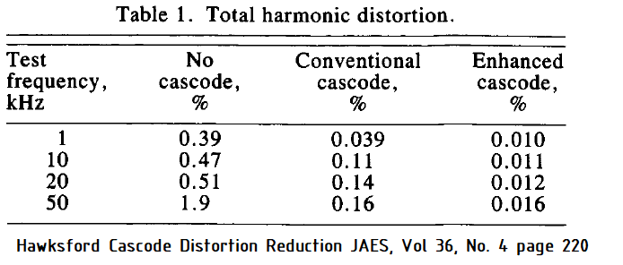
Malcolm Hawksford published an article in the JAES, Vol 36, No. 4, in 1986 on "Reduction of the Transistor Slope Impedance Dependent Distortion in Large-Signal Amplifiers". He coupled the current coming out of the base of the Cascode output transistor to the Cascode's "bottom" transistor's emitter. This generated a local feedback loop that raised the output impedance of the Cascode and reduced the distortion of the Cascode. I've redrawn his circuit below.
In the Hawksford's article, he published the following distortion improvements in his test circuits. The improvements are impressive.
There Ain't No Such Thing As A Free Variable (or Free Lunch)
I find that the Hawksford Cascode likes to oscillate in the 10s of MHz region if you aren't super careful. With a PWB, the Hawksford Cascode can be made to work in the MHz region, but it takes effort to make it happen.
I've also found that SPICE doesn't always predict Cascode oscillations correctly. This is mostly because we don't have all the wiring and trace parasitics in the SPICE model.
For Audio frequencies, the best solution I've found so far is to add 2 resistors and a cap to turn it back to a conventional Cascode at high frequencies. I normally set the resistor in the RC Damper to be equal to or down to 1/4 of the "Grid Stopper" resistor value. The RC damper needs to look like a resistor at 1/2 or lower than the frequency where the oscillations/ringing occurs.
With MOSFETs, I normally see the capacitor in the RC Damper being equal to or slightly larger than the Ciss of the MOSFET. If you don't like the performance with the RC damper, work with the part and trace positions and add a "Grid Stopper" to the lower FET, this can let you lower all "Grid Stopper" values and then you can re-tune the RC damper.
With MOSFETs, I have found that you want the drain voltage of the "bottom FET" to be at least 2V higher than the gate voltage. As the drain voltage approaches the gate voltage, the MOSFET's internal capacitances tend to steeply rise.
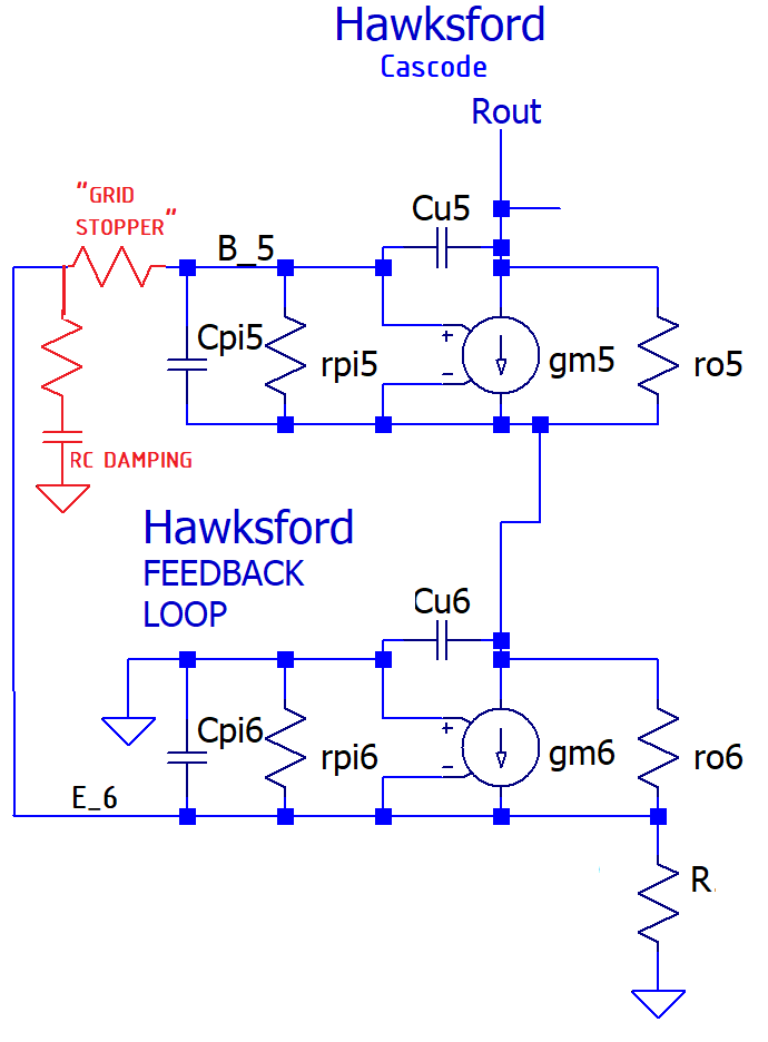
The "RC DAMPING" goes to the "AC Ground" of the Cascode. This is the local reference "Ground" where "R" attaches. This ground is often not Chassis Ground. It occasionally can be Signal Ground. For PNP Transistors, this ground could be B+.
Ground can be a transcendental topic. I have worked with the "AC/Signal ground" being -1200V to +3000V away from Chassis Ground. In my snarkier moments, I've been known to claim there is only one electron in the universe that is actually "ground." All other grounds are referenced to it, but with some error. I keep this ground taped to the back of my phone under the phone case, so I always know where it is. You can look at my electron, but you can't touch it! ;-} With less "Snark", I have circuits where I've made 4V spikes in 2 paralleled ~1 inch wide ~2 inch long ground traces. So, Ground really isn't always at 0V.
From the Spice Model with the tubes pulled at 318V on B+, each amp will draw 5.88mA and the effective load resistance for two channels of amps on B+ is 27Kohm.
From the Spice Model with the tubes installed, nominal Gm, at 318V on B+, each amp draws 51.6mA for an effective load resistance for two amps of 3.041Kohm.
Plopping this data into both Excel and Duncan Amps PSUDII Link. We can design our power supply.
Typically, the rated current for the high voltage secondary needs to be 2.5 times the DC output current.
The needed RMS voltage on the secondary runs between 1/1.30 to 1/1.12 times the needed DC voltage. This puts us in the range of an inexpensive 115V to 230V rated transformer.
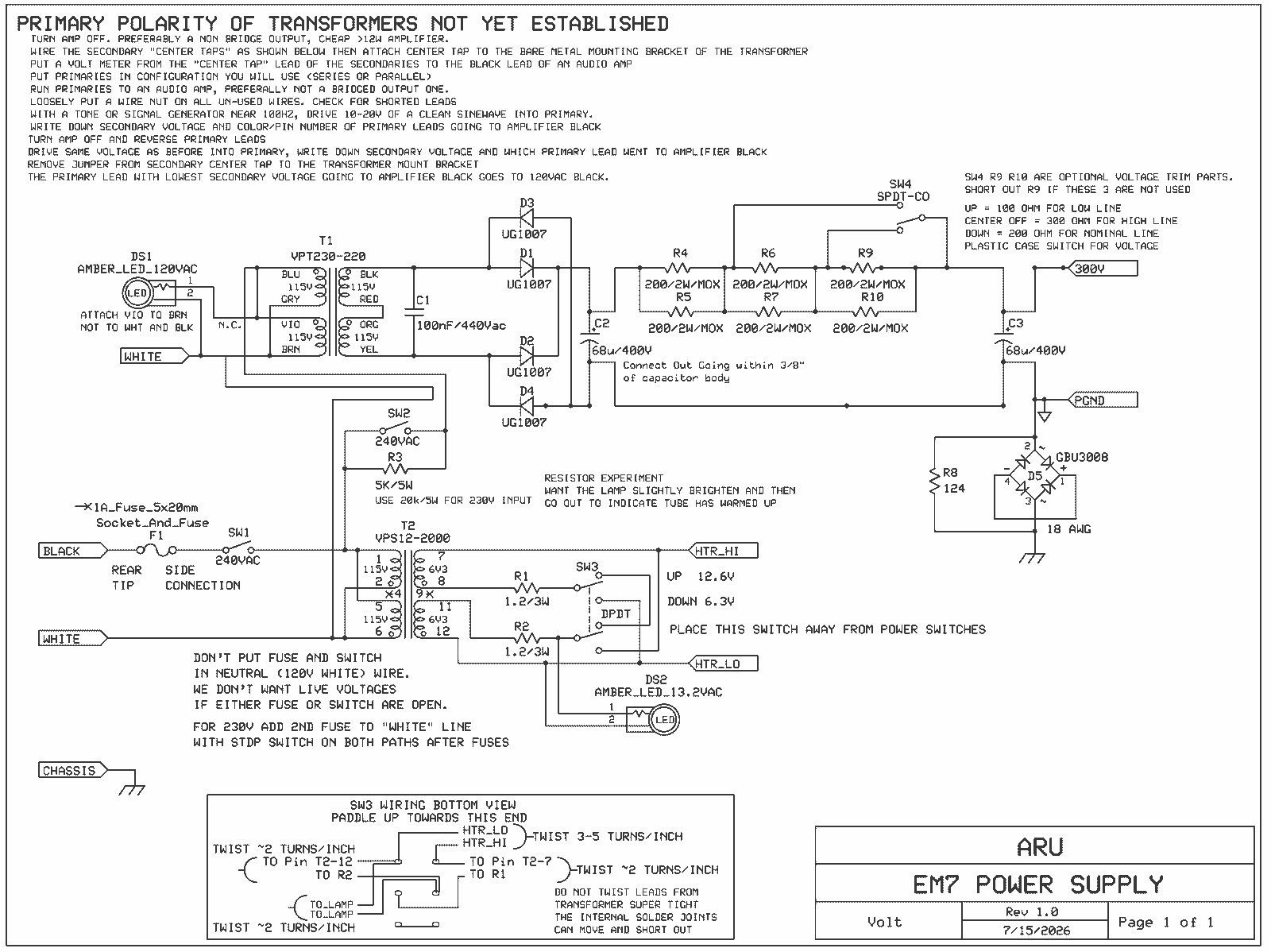
I would like to switch the HV on separately from the filament. I'll use the filament switch to "enable" the high voltage switch. I want to try a trick and have one power on LED for the filaments and one for the high voltage. If I set the high voltage power on switch up correctly, it will reach half brightness over a few seconds and then dim to 1/4 brightness when the filaments are warmed up. From what I've heard, 1/2 rated B+ with a cold filament isn't very risky for most non-mercury low voltage tubes (i.e. <<1kV plate).
I'd also like to trim the B+ based on +/- 5% line voltage regulation. Roughly speaking, a 5% change in B+ gives a 10% power loss change in the tubes.
Make the solder joint to the aluminum capacitors about 1/4 inch from their rubber gasket. Don't use chlorinated solvents or water to clean the flux/grim off of the aluminums. Chlorine catalytically kills aluminum electrolytic capacitors (the chlorine doesn't get used up in the reaction.)
The parts list does not include the case, screws, star washers, nuts, glue and terminal strips needed to build this.
|
Qty |
Name |
Order |
Part |
|
1 |
100nF/440Vac |
399-R474N310050A1KV057-ND |
C1 |
|
2 |
68u/400V |
1189-400LXW68MEFR12.5X30-ND |
C2,C3 |
|
1 |
AMBER_LED_120VAC |
1092C3-125VAC-ND |
DS1 |
|
1 |
AMBER_LED_13.2VAC |
458-FL1P-10NW-2-Y12V-ND |
DS2 |
|
1 |
GBU3008 |
3757-GBU3008_T0_00601-ND |
D5 |
|
4 |
UG1007 |
31-UG1007_HF-A52CT-ND |
D1,D2,D3,D4 |
|
1 |
Socket_And_Fuse |
Q205-ND |
F1 |
|
2 |
1.2/3W |
13-PNP300JR-73-1R2CT-ND |
R1,R2 |
|
1 |
124 |
13-MFR-25FRF52-124RCT-ND |
R8 |
|
6 |
200/2W/MOX |
RSMF2JT200RCT-ND |
R10,R4,R5,R6,R7,R9 |
|
1 |
5K/5W |
A142817CT-ND |
R3 |
|
2 |
240VAC |
708-3049-ND |
SW1,SW2 |
|
1 |
DPDT |
2057-SW-T2-4B-B-A2-MA2-ND |
SW3 |
|
1 |
SPDT-CO |
2449-AST13SEBQ-ND |
SW4 |
|
1 |
VPS12-2000 |
237-1256-ND |
T2 |
|
1 |
VPT230-220 |
237-1331-ND |
T1 |
|
1 |
1A_Fuse_5x20mm |
0234001.MXBP-ND |
Z1 |
|
1 |
AMBER_NEON_120VAC |
6088-WL-1030D3-ND |
ALT_DS1 |
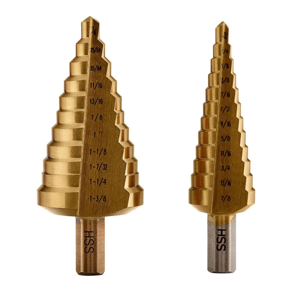
Drill all holes first with a pilot hole into a divot made with a center punch. Slowly enlarge the hole to the size needed with a stepped drill bit using a little oil. I borrow some Olive Oil from the kitchen if my bottle of machine oil is misplaced. With this method, the holes come out consistently round with very little damage and bending to the chassis.
One other restriction, we want the high line no tubes installed voltage to be less than 400V. I don't want to have to lower the value (uF) in all of the high voltage capacitors to use a 450V or 500V capacitor. This rules out the Triad VPS line of parts that have 25% regulation.
The Triad VPT230-430 Digikey 237-1338-ND for $48.51 looks good. For Duncan Amps inputs we use:
T1 nominal voltage is (120V/Primary rating of XFMR)*Rated Secondary Voltage * (1 + Regulation factor) or 120V/115V*230V*(1 + 9%) = 261.6Vac. Maximum High line is 10% higher (287.8Vac).
T1 output resistance is Nominal Rated Secondary Voltage * Regulation Factor / Secondary Rated Current. 230V*9%/0.43A = 48.14 ohm
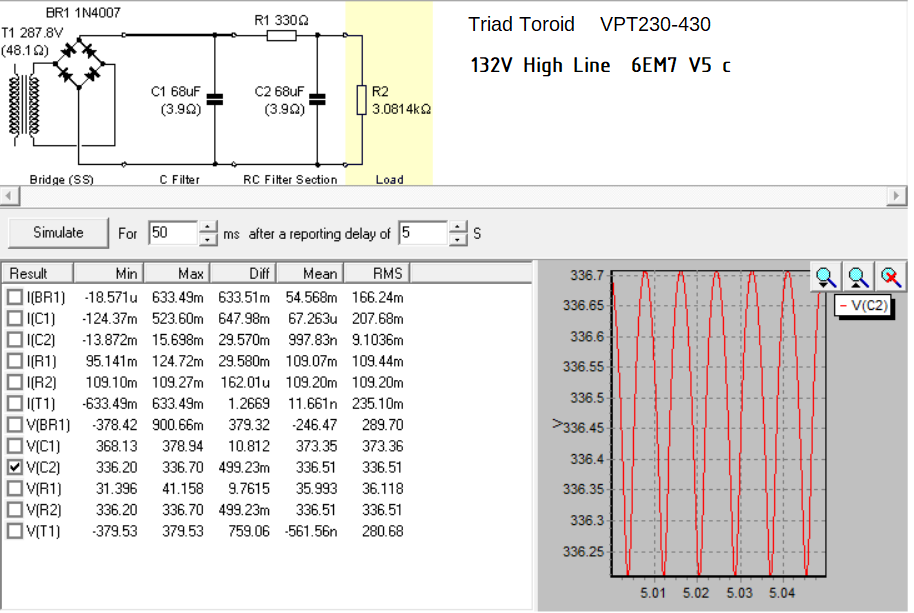
The Triad VPT230-220 Digikey 237-1331-ND for 37.01 will also work, but it will run on the hot side, but it will run in its allows temperature rise. If using this transformer, I'd change all the 330 ohm 2W MOX resistors to be 200 ohm 2W MOX resistors to keep the voltages the same. Unloaded at 132Vac input, this will run 2V higher than 400V. This is 0.5% over specification in an edge condition, while I'd rather have the margin, we should be able to live with it.
Use 600 to 1200V >=1 amp fast diodes or ultrafast diodes in the diode bridge. Ultrafast diodes normally have a lower surge rating than fast diodes so you want to double-check the surge current rating with them. The VPT230-430 will only need a 5A 8.3msec surge rating (or 0.208 A^2*sec I^2*t). A UV4007, Digikey UF4007CT-ND, will work here.
Use the same 68uF 400V capacitor as used in the amplifier for the first capacitor after the diode bridge.
I recommend a snubber across the secondary. Because the current margin in the smaller transformer is low, we don't want too large of one. A capacitive draw of 10% of the secondary load would be acceptable. The capacitor current draw is out of phase with the main current flow in the transformer and normally will not cause a significant increase in power loss. The value would be 230V/.22A * 10 = 10.45K ohm at 60 Hz, or less than 0.25uF rated at 300Vac or higher (the unloaded voltage of the transformer). A 0.068uF 310Vac (used in the amp section) should work good enough.
In a tabular format, here is what we have.
|
132.0 |
High Line |
|
120.0 |
Nom Line |
|
126.0 |
Mid Line |
|
27015.1 |
Rmin load |
|
3081.4 |
Rmax load |
Parameters for Four transformers (more exist)
|
Manufacture |
Model |
Vin |
Vout |
Iout |
Regu- |
Temp |
Rout |
V Xfmr
RMS |
V Xfmr |
V Xfmr |
V Xfmr |
15 July |
|
Triad A |
VPS230-350 |
115 |
230 |
0.35 |
0.25 |
30 |
164.3 |
300.0 |
315.0 |
330.0 |
285.0 |
$31.25 |
|
Triad Toroid |
VPT230-430 |
115 |
230 |
0.43 |
0.09 |
45 |
48.1 |
261.6 |
274.7 |
287.8 |
248.5 |
$48.51 |
|
Triad Toroid |
VPT230-220 |
115 |
230 |
0.22 |
0.12 |
40 |
125.5 |
268.8 |
282.2 |
295.7 |
255.4 |
$34.91 |
|
Signal |
A41-80-230 |
115 |
230 |
0.35 |
0.10 |
TBD |
65.7 |
264.0 |
277.2 |
290.4 |
250.8 |
$36.23 |
VPS230-350 goes too high in voltage with a cold tube. I didn't bother to try to optimize
|
Triad A |
uF cap |
ESR |
Line |
Rload |
Voltage |
Amps |
Amps Xfmr |
330ohm |
Vpp 2nd cap |
Vcap 2 |
|
VPS230-350 |
6.80E-05 |
3.9 |
132 RMS |
27015.1 |
445.25 |
n/a |
n/a |
439.8 |
n/a |
1.380 |
|
|
|
|
132 RMS |
3081.4 |
388.89 |
0.169 |
0.204 |
350.5 |
0.463 |
1.100 |
|
|
|
|
126 RMS |
3081.4 |
|
|
|
334.6 |
|
1.050 |
|
|
|
NOM |
120 RMS |
3081.4 |
|
|
|
318.7 |
|
1.000 |
VPT230-430 has promise, but suddenly, part availability went to zero at both Digikey and Mouser.
|
Triad Toroid |
uF cap |
ESR |
Line |
Rload |
|
Amps |
Amps Xfmr |
330ohm |
Vpp 2nd cap |
Vcap 2 |
|
VPT230-430 |
6.80E-05 |
3.9 |
132 RMS |
27015.1 |
398.15 |
n/a |
n/a |
393.2 |
n/a |
1.286 |
|
|
|
|
132 RMS |
3081.4 |
373.35 |
0.208 |
0.235 |
336.5 |
0.499 |
1.100 |
|
|
|
|
126 RMS |
3081.4 |
356.33 |
0.198 |
0.224 |
321.2 |
0.476 |
1.050 |
|
|
|
NOM |
120 RMS |
3081.4 |
339.36 |
0.189 |
0.214 |
305.9 |
0.453 |
1.000 |
VPT230-220 will work, but will run on the warm side. It is available at both Digikey and Mouser. I ran the numbers with a 330 ohm B+ dropping resistor. 200 ohms is a better choice.
|
Triad Toroid |
uF cap |
ESR |
Line |
Rload |
|
Amps |
Amps Xfmr |
330ohm |
Vpp 2nd cap |
Vcap 2 |
|
VPT230-220 |
6.80E-05 |
3.9 |
132 RMS |
27015.1 |
401.91 |
n/a |
n/a |
397.0 |
n/a |
1.352 |
|
|
Rseries 330 |
|
132 RMS |
3081.4 |
358.35 |
0.165 |
0.196 |
323.0 |
0.440 |
1.100 |
|
|
Rseries 330 |
|
126 RMS |
3081.4 |
342.04 |
0.157 |
0.187 |
308.3 |
0.420 |
1.050 |
|
|
Rseries 330 |
NOM |
120 RMS |
3081.4 |
325.75 |
0.150 |
0.178 |
293.6 |
0.400 |
1.000 |
|
|
|
|
114 RMS |
3081.4 |
309.51 |
0.142 |
0.169 |
279.0 |
0.380 |
0.950 |
VPT230-220 can be tuned up for better performance by changing the resistor value between the 1st cap and 2nd cap. You don't have to do this tuning. You could just use one resistor value and live with any line variation. I'm having fun here so I will likely do it on my first build. The switch doesn't make a huge change in the B+ static regulation, but I'll take the improvement it does provide.
If you tune the B+, you don't have to do it tuning with a switch; but you can. I saw someone do this with a lead wire and a spade lug inside the amp, and they moved the spade lug to pick the resistor value they wanted. This is dangerous. You must be 100% sure the B+ and line voltage are at 0V when you move the wire. If using a chassis mounted switch, you can change value with the 115V on.
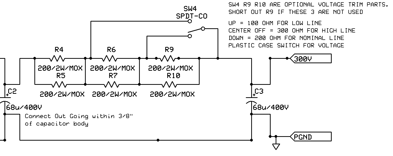
|
Variable Rseries in PSU |
|
Line |
Rload |
|
Amps |
Amps Xfmr |
330ohm |
Vpp 2nd cap |
Vcap 2 |
|
|
VPT230-220 |
Rseries 100 |
|
114 RMS |
3081.4 |
307.06 |
0.115 |
0.178 |
296.7 |
1.194 |
0.976 |
|
VPT230-220 |
Rseries 200 |
NOM |
120 RMS |
3081.4 |
324.39 |
0.153 |
0.183 |
303.9 |
0.663 |
1.000 |
|
VPT230-220 |
Rseries 300 |
|
126 RMS |
3081.4 |
341.68 |
0.158 |
0.188 |
310.7 |
0.461 |
1.022 |
I didn't run the numbers for the Signal transformer, but it looks viable. If I were using a higher DC bias current on the output tube, I'd probably use it and adjust the dropping resistor values and wattages in the PSU.
If we select a filament transformer that has two 6.3V secondaries, we can add a simple switch to choose a 6.3V tube or a 13V tube.
The required Filament Powers are as follows:
13V +/- TBD 0.450A per tube for 13EM7 Pins 7 and 8. This is 0.90A for two tubes (i.e. 12.6V with 11 seconds warm-up time.)
6.3V +/- 10.% 0.925A per tube for _6EM7 Pins 7 and 8. This is 1.85A for two tubes. (6.3V/ 0.925A = 6.81 ohm per filament)
I would use a dual secondary transformer with a 6.3V rating per winding at greater than 2.5A parallel current rating. The 2.5A rating will result in a cooler transformer. If the secondary voltage runs high, correct it with a Stepped Autoformer for 120V or add a wire wound resistors in series with the each of the windings going to the switch (one resistor per switch solder joint).
With a filament transformer, poor load regulation (25% vs 10%) has a side benefit of providing inrush current limiting to the filament as the heater warms up. At the same gauss drive, a transformer with 25% regulation runs hotter than the same output power transformer with 10% regulation. But the 25% regulation transformer MAY have traded lower core loss for higher copper loss. The datasheets don't give use that data. For more info, see Lowell Quist's Article on Regulation Based Transformer Design.
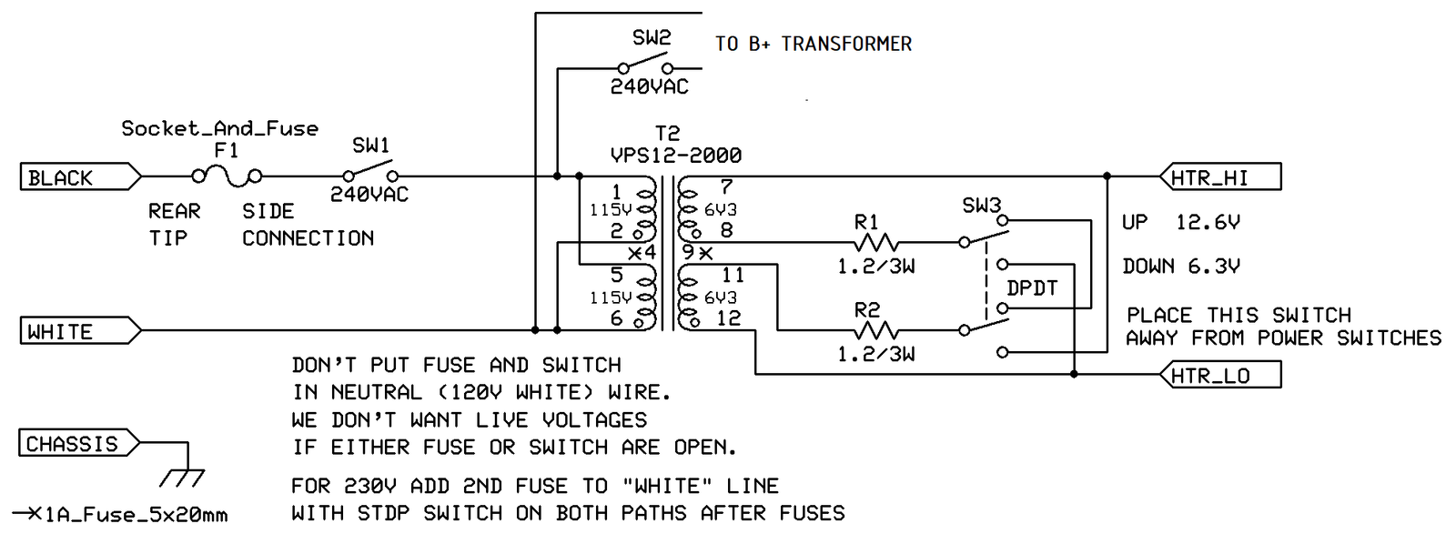
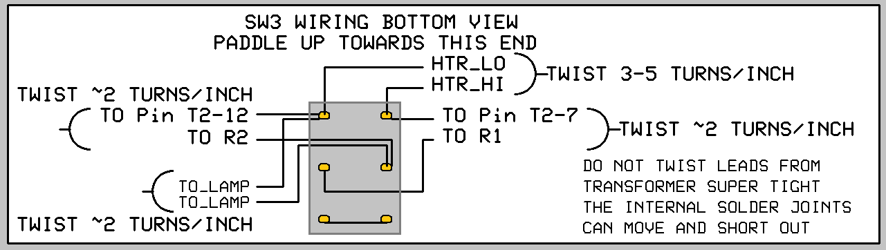
The switch wiring can be confusing. Below is what we want.
I'd place a lamp on one of the 6.3V windings to indicate that filament power is on. The lamp voltage should always be 6.3V in either switch position. Many lamps are too bright for my tastes, so I'd use a 12V lamp for this function and put 6V on it to make it not as bright.
The other end of R2 goes to T2-11. The other end of R1 goes to T2-8.
The Hammond 266JB12 $38 is 6.0V per winding out at 1.2A at 117V input. Increasing the line voltage to 120V gets us to 6.15V. I would "guess" the line regulation of this part is 12% for an open circuit voltage of 6.15V*1.112=6.89Vrms with a series resistance of 6*0.12/1.2=0.6 ohm. 6.89V - 0.925A load * 0.6 ohm = 6.33V. It will work.
The cheaper Triad VPS12-2000 $16.13 is 6.3V at 2.0A per winding at 115V input with 25% regulation (30C typical, 45C max rise). 120V input brings us to 6.574V. 25% regulation brings the unloaded voltage up to 8.217V. 25% regulation is 6.3*0.25/2A = 0.7875 effective ohms in the secondary.
8.217V * 6.81 ohm filament/(6.81 ohm + 0.7875 ohm transformer) = 7.36V out under the filament load. To get 6.3V out, we'd want to put a 1.2 ohm 3W wire wound (or 5W MOX) in series with each 6.3V winding. Possibly use a Yageo PNP300JR-73-1R2 Digikey 13-PNP300JR-73-1R2CT-ND at $0.43 each. This part is surge rated for 10X rated power for 5 seconds (150 joules) with a 2% value change from the surge. We'll be running an estimated 3.8X rated (assuming 10% of Rnom for a cold filament) for about 7 seconds during filament warm up (80 joules). If in the actual build we miss the filament voltage by more than 5%, I'd adjust the resistor value. The raw power line voltage is normally +/- 5%, I'm used to seeing closer to +/- 10%.
A Zip of files used in this presentation.
First
version 20-July-2026, Last update 20-July-2026
Changes to
correct font or spelling issues won't count as an update.
.
 (
New 2024 index page.)
(
New 2024 index page.)
 _(
Old 2003 index page.)
_(
Old 2003 index page.)
 _(
AMP Second index page.)
(
Fancy index page.)
_(
AMP Second index page.)
(
Fancy index page.)
.