
What is "OFF" for a Bipolar Transistor?
What does it take to turn off a transistor?
The quick answer is to be "OFF":
You will need less than 145K from Base to Emitter with an "ideal" resistive input drive just to deal with Icbo. Off being 1.93uA Collector Current at 95C Tj, not T ambient.
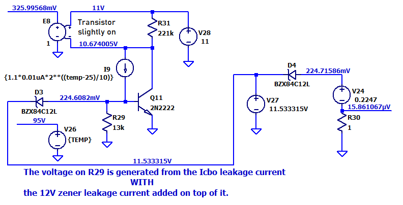
To deal with Icbo and the leakage from a typical 12V Zener, you'll need less than 13.1K Base to Emitter .
5. What else is there to be nagged about?
=================
Before we talk transistor math, first a "Tube Nerd" joke:
No, you can't turn a transistor "Off" by just yelling at it "Your Mother was made from sand with fleas in it."
. . . Tube aficionados call transistor amps "Sand Amps"
. . . So if we insult the pedigree of the parts in the amp, the parts will turn off. . .
Oh well, if you have to explain the joke you need to keep your day job.
=================
"OFF" can be considered when the total collector current is approximately twice the collector to base leakage current (Icbo). The choice to set the collector current equal to the Icbo current is an arbitrary choice, but from experience, setting it lower than this makes the design process difficult. This low collector current plus the transistor's temperature rise results a very low Vbe for the transistor to be "OFF." This low Vbe voltage working against the Icbo and other external current flowing into the base junction results in the need for moderately low resistor values across Vbe to insure the transistor always turns "off."
A simple LTSPICE example is shown below. At 100C junction, the transistor turns on (or would fail to turn off) with 221K from base to emitter (middle picture) and is "almost" off with 100K base to emitter (right picture). Look at the voltage across the 221K resistor in the collector to see what I'm talking about. Lowering the ohms from base to emitter lower than 100K or operating with a lower junction temperature help solve this issue.

Don't assume the junction temperature is going to be super low (<85C.) First it is the junction temperature that counts, not the ambient or case temperature. Second, is you need to plan for a hotter than "what you think" environments. A 65C air temperature with a 30C rise over "ambient" gets you to 95C. A hot part next to your "sensitive BJT" can also raise the temperature of the BJT. In short, the top of your electronics may be at 45C, that doesn't make the "ambient" air inside the box that cool and definitely, the BJT junction isn't running that cool.
45C case temperature + 20C internal temperature rise around the part + 200mW/C Rthja * 150mW of loss (30C) = 95C
Icollector = Hfe * Ibase
Ibase = Io * (
e^(Vbe/(nkt/q))-1) where nkt/q is typically 26mV. and we
don't worry about the "1". 26mV more across Vbe gives 2.7 times
more current.
Icbo =
Collector to Base current with Emitter open. This unwanted
current typically doubles every 10C of junction temperature.
Not related to this analysis, but the "Early Voltage" for transistors is not specified in datasheets. When you draw the curves for the BJT, the Early voltage is where the slopes of all the curves of a curve sweep intersect "zero current." This early voltage determines the parallel resistance from collector to emitter on the BJT. This is different than the plate resistance of a tube which is in series with the tube's output, this resistance is in parallel. One reason we care about this is that the Early voltage is it sets how good of a current source you can make with a transistor and limits how much low frequency power supply rejection we can get from a circuit.
The models used in SPICE are a model. They are not an actual part. The manufacture sells you a part to the DATASHEET's performance table, not the SPICE model and not to the typical curves in the datasheet. I've had friend's design stop working in the factory because of parts coming in just barely met the datasheet limits because purchasing found a lower price source (seriously, purchasing did their job right) for the part. This happened because my friend designed to the "nominal" curves for the part (oops.) Even with taking lab test data to validate those nominal curves, it is a risk. I actually did this once myself the first year out of college (with a 5.1V zener). I got severely chastised by my boss and was told to go fix it before I went home (it was a long week.) After that, I made an major effort to not repeat that mistake.
The Collector to base breakdown voltage is not modeled in SPICE. You can put 10kV across a 40V transistor and SPICE won't flag an error. Collector voltage breakdown is mostly a "thermal damage" risk which is made worse with a possibility of hot spotting inside the BJT. Vcb (collector to base) breakdown should be avoided, but not to the extent of the Vbe (base to emitter) breakdown voltage has to be avoided.
The Base to Emitter breakdown voltage is also not modeled in SPICE. This voltage is normally rated between 5-7V. This breakdown is not a avalanche type of breakdown. Vbe breakdown often degrades the noise and current gain of a BJT. Back before decent FETs were available for switching power supplies, high current BJT used for switching were reversed avalanched (pushed into Vbe breakdown) to turn them off quickly and the designs just planned on the Hfe dropping from the abuse. What about the noise figure increase in these power switches? No one cares about that. The part was to be either on or off.
SOA (Safe operating area) is also missing from SPICE. For us "humans", the most common mistake using the SOA is not correcting for the case temperature. SOA is normally specified with case temperature held at 25C. If Tj is rated for 150C and the case is at 75C, only (150C - 75C)/(150C-25C) = 0.6 of the datasheet's SOA current can be used.
I normally like to keep my worst junction temperatures far below 95C and my box temperatures below 65C. For reference, 65C is your car's summer steering wheel temperature in Phoenix on the days you forgot to put the metalized bubble pack window shade in the front window. Between 105C and 125C something not good happens in a BJT, I don't remember what it is at the moment. It isn't great, but it isn't horrible either. Above 125C something else kicks in that is worse that what happens at 105C. Again, I don't remember what it is. If I ever do, I'll update this page or write a new one. If you have a part that has a variable temperature rise due to its power loss changing several times a minute, keep the temperature VARIATION low (~10C.) This is to avoid degrading solder joints and other items from the temperature cycling.
Public domain reference documents:
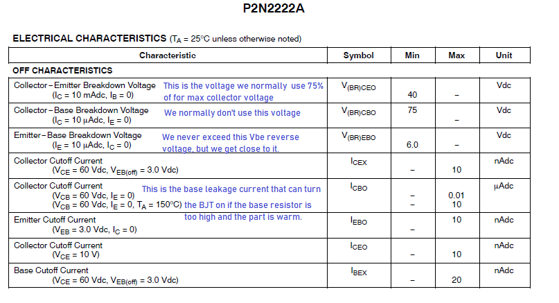
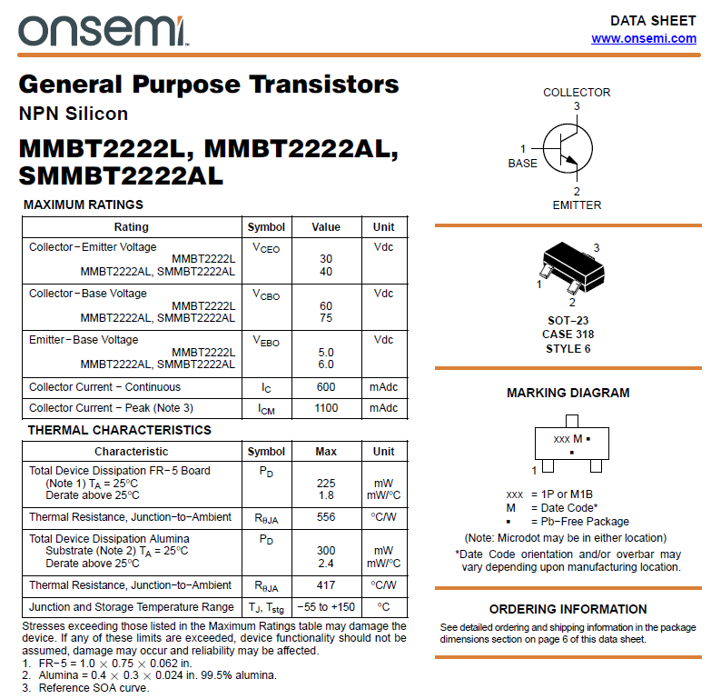
Here is a typical data sheet from Onsemi:
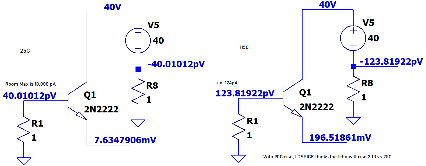
Below is what the SPICE model thinks Icbo will measure.
Spice thinks Icbo is 250 times lower than what the datasheet allows and doesn't change as much with temperature.
The data sheet is what the manufacture can sell you and meet still the
controlling requirements in the datasheet. The manufactures are also
allowed to make parts that work much better the the datasheet, hence the
"nominal" models that make it to "SPICE." If Icbo is a critical parameter
in your circuit and both SPICE and the first one you build works, but you
didn't do a full analysis, the 67th circuit you build may not work.
I'm showing 115C in examples to encourage you not to let your parts get
that hot. I don't like running my junctions that hot. SPICE says
there it nothing to worry about, but there is.
For analysis, the normal assumption is that the Icbo leakage current (base leakage current) doubles every 10C. Lets check this out against the PN2222A datasheet with listed values at 25C and 150C..
Ileak_hot = Ileak_25C * N1^( (150C - 25C)/10C) (N1 (the "base" of the exponential function is normally "2")
Ileak_hot/ Ileak_25C = N1^( (150C - 25C)/10C)
Ya gotta love the rules of logarithms! Lets use them to solve for N1.
log(Ileak_hot/ Ileak_25C) = log(N1^( (150C - 25C)/10C))
log(Ileak_hot/ Ileak_25C) = (150C - 25C)/10C) * log(N1)
log(Ileak_hot/ Ileak_25C) / (150C - 25C)/10C) = log(N1)
log(10u/0.01u) / (12.5) = log(N1) ( knowing (150C - 25C)/10C) = 12.5 )
240E-03 = log(N1)
10^240E-03 = N1 = 1.7378 = the "BASE" of the exponential function.
Checking 0.01uA * 1.7378^(12.5) = 10uA. Yes, the math checks.
So for this part, leakage current doesn't double every 10C, it goes up by 1.7:1. I've run this calculation on other parts and actually came up with just under 2:1 for every 10C for most of them. I'll stick with the doubling every 10C because it is what I see more often than the 1.7 number. Later, we'll look at a different datasheet and it will have a BASE of "2" like what it normally should be.
At 115C, we'd expect Icbo to be
0.01uA * 2^( 115C - 25C)/10C) = 0.01uA * 2^9 = 5120nA. That's a pile more than 123.8pA given in SPICE.
Increasing Icbo by 10% for EOL = 5630nA. That's 5.6 uA into the Vbe's base node. That's a lot more than the 123.8picoamps SPICE predicted. (Yes, I nagged twice.)
How much base current will be needed drive an equivalent 5630 nA in the
collector? We'll have to be pessimistic here and assume that worst
case the Hfe doesn't drop between 150mA and 1uA. This base current
reduces the Icbo flowing out of base of the transistor. It helps us,
but it is worth considering considering how complex this math is getting?
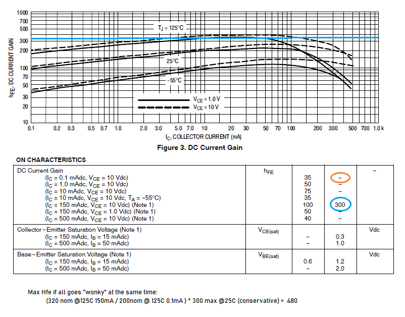
I base to drive 5.6uA collector current would be 5630nA / 480 = 11.7nA for driving the Icbo collector current. 11nA is nothing (0.2%) compared to 5630nA. Lets ignore it and make the math simpler.
Don't weasel out and use a lower the junction temperature that occurs just before power up or at light load on a cool day! When we go to turn the transistor off, it will be HOT, it hasn't cooled off yet. For all we know the circuit could be in a nice looking wood cabinet with 7 other circuits with no air circulation instead of being on top of a workbench in open air. We have to use the maximum "in use" and "in test" allowed HOT junction temperature to figure out leakage currents, not the ambient temperature.
What would Vbe at HOT be? We will care about that.
At 25C 0.1mA Ic, Vbe per the ONSEMI P2N2222A/D January, 2013 Rev. 7 data sheet is 0.55V with a temp co of =2.2mV/C
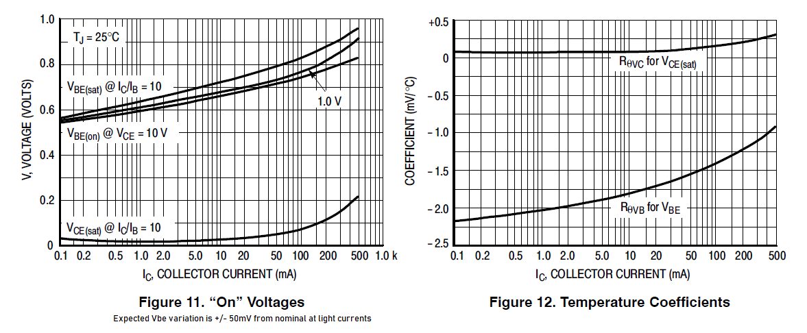
At 25C, LTSPICE results show 597mV not 550mV for 0.1mA of collector current. (The little bit of base current flow isn't significant in this example.):
Per LTSPICE, the 2N2222A at 0.1mA at 25C, Vbe is 0.597V, this is 64mV higher than the ONSEMI Datasheet. The ONSEMI datasheet also says Vbe should change -2.2mV/C where the LTSPICE model changes -2.0mV/C. We just saw proof that the model and the datasheet don't always track each other.
Knowing the diode equation and the magic of Logs, lets do a lot of math:
Id = Io*(e^(Vbe/(nkt/q)) - 1 ) ( Just drop the -1, it is small compared to the other number, e^(200mV/26 mV) = 2191 )
Id1 / Id2 = (e^(Vbe1/(nkt/q)) ) / (e^(Vbe2/(nkt/q)) ) = e^((Vbe1-Vbe2)/(nkt/q))
Ln (Id1 / Id2) = (Vbe1-Vbe2)/(nkt/q) = (Vbe1-Vbe2)/26mV
26mV * Ln (Id1 / Id2) = (Vbe1-Vbe2)
26mV * ln(5630nA/0.1mA) = 26mV * -2.87 = -0.0748V delta V from current ratio
Vbe = 0.55V @ 0.1mA - 50mV variation + (115C-25C)*-2.2mV/C - 0.0748V leakage dV
Vbe = 0.55V @ 0.1mA - 50mV variation - 198mV temperature - 0.0748V leakage dV
Vbe = 0.302V - 0.0748V leakage dV = 227mV = Which is a bit tiny.
To be less pessimistic on the leakage current, we could:
A. Assume 25mV matching to datasheet nominal instead of 50mV.
B. Making the base current needed to generate the collector current less pessimistic doesn't help enough to really do much.
Hfe 35min datasheet * (105 @ 0.1mA 25C/35 min data sheet) * (205 @ 0.1mA 125C/105 @ 0.1mA 25C) = 205 Hfe vs 480. . .
Vbe = 0.55V @ 0.1mA - 25mV variation + (115C-25C)*-2.2mV/C - 0.0748V leakage dV
Vbe = 0.252V, Still tiny.
A "nominal LTSPICE model at 115C gives 0.311V for Vbe with Ic = 11.26uA with 5630nA of that being the base leakage in the Ic. (See below) This is 59mV different from the calculated number.
If LTSPICE matched the datasheet at 25C, we'd be at 0.311V - 23mV - 47mV = 241mV. This is closer to the 227mV number we got assuming 50mV match to the datasheet instead of 25mV. The 227mV for Vbe doesn't seem that far fetched now. BUT, I'll stick with 0.252V (25mV to curve) mostly because the next few pages of math are already done and spell checked and I don't want to re-do them.
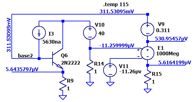
( Above is a circuit to force a given collector leakage current by varying the Vbe voltage.)
You want a bigger allowed Vbe?
If we allow the collector leakage current to be 60uA instead of 11.3uA (voltage on R14), SPICE tells us the base voltage rises from 0.311V to 0.387V. If the base of Q6 was also driven through a zener that had just less than 60uA of leakage current, we could use a 5.11K resistor base to emitter to keep the transistor off (i.e. 60uA of current at base node with 60uA of collector current allowed feeding next circuit)
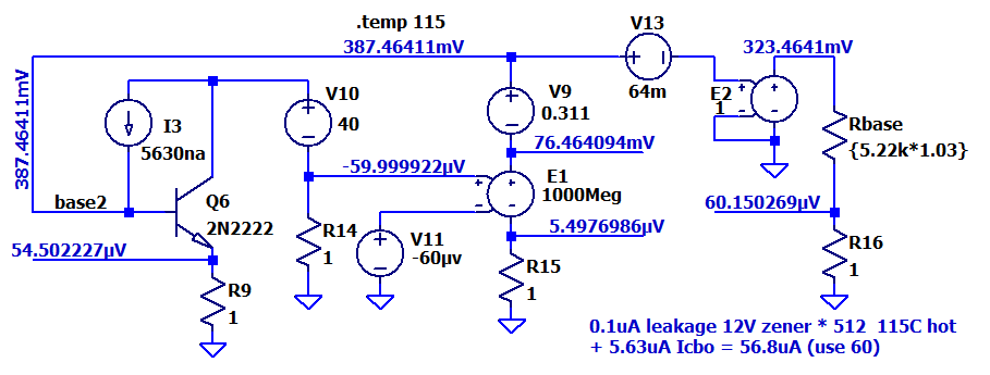
Decreasing the temperature helps at any collector current.
At 95C vs 115C at Ic = 11.26uA, the allowed Vbe off voltage is better, 0.375V @ 95C vs 0.314V @ 115C.
At 95C vs 115C at Ic = 60uA, the allowed Vbe off voltage is better, 0.432V @ 95C vs 0.387V @ 115C.
At 95C the allowed Vbe off voltage at an Ic current 60uA Ic total is better, 0.432V vs 0.375V at 95C with Ic = 11.26uA.


An example of why we care about the off current in the collector follows. If the collector of the transistor drives an AC Schmitt gate that normally runs from 5V but must "work" during power down at 3.0V Vdd, the gate will need 0.8V between the gate input and Vdd for the output to have the correct state (see datasheet info below.) At 115C with 60uA of collector leakage current from the transistor being off, this means the pull up resistor on the Schmitt gate must be
0.8V/60uA/1.03 = 12.9K ohm.
If we designed for 11.26uA of collector leakage (5.6uA Icbo + 5.6uA Ic) current at 95C, this resistor could be
0.8V/11.26uA/1.03 = 68.9K.
That is a substantial difference. If we design Vbe resistor to pull Vbe to a lower voltage, the collector current will drop more allowing even a higher pull up resistor.

At 115C, the maximum Base-Emitter resistor to turn the 2N2222A off (off = 11.2uA collector current) would be
Rbe max = 0.227V (Calculated,50mV match)/5.63uA/1.03 tolerance = 39.1 Kohm if driven from a perfect switch. If you find a perfect solid state switch, email me!
What happens if another transistor drives the Vbe? The Rbe will have to sink 3X more current (the Icbo from itself + the Icbo of the drive part + allowed collector current of it's driver)
Rbe max = 0.227V (Calculated,50mV match)/(3*5.63uA)/1.03 tolerance = 0.227V/16.9uA/1.03 tolerance = 13 Kohm (Not shown in the spreadsheets below)
What happens if zener leakage of 56.3uA drives the Vbe? The Rbe will have to sink 56.3uA from the zener + 5.63 = 61.93uA. (Off = 11.2uA collector current)
Rbe max = 0.227V (Calculated,50mV match)/(61.93uA)/1.03 tolerance = 0.227V/61.93uA/1.03 tolerance = 3.56 Kohm ( Hey! it matches the PN2222A Excel sheet below! )
What happens if if we use the same zener and transistor at 95C and the leakage currents drop to 14.08uA for the zener and 1.4uA for Icbo (15.49 uA into the base node.)
Rbe max = 0.271V (5.6uA Ic over Icbo, Spreadsheet)/(15.49uA)/1.03 tolerance = 16.99 Kohm ( This is a value that is nice in several of my circuits that are on the drawing board.)
Ah, the crazy games we need to play when we just can't throw away current everywhere in the circuit. . .right?First lets take all the math from the first example and put it into Excel. Excel File For Calculations
The bottom array of numbers has a sliding scale of extra current into the base that will add to Icbo. This extra current matches the leakage current from a zener.
The MMBT2222A (should be the same as a PN2222A) is specified at 10uA leakage "HOT" where HOT is 125C not 150C as for the PN2222A.
The Vbe curves for the MMBT2222A only go down to 1mA, not 0.1mA.
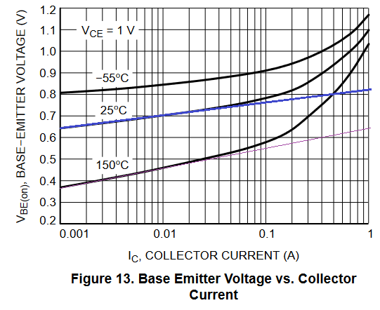
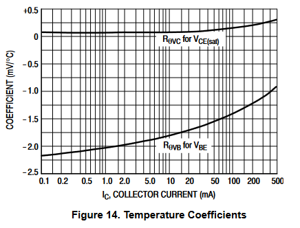
At 115C, the maximum Base-Emitter resistor to turn the MMBT2222A off (off = 11.2uA collector current) would be 44.4K ( not 39.1K with the PN22222A data)
What happens if zener leakage of 56.3uA drives into the Vbe along with Icbo? The Rbe will have to sink 56.3uA from the zener + 5.63uA Icbo = 61.93uA. (Ic Off = 11.2uA collector current)Rbe max = 0.257V (Calculated,50mV match)/(61.93uA)/1.03 tolerance = 0.257V/16.9uA/1.03 tolerance = 4.03 Kohm ( Hey! it matches the MMBT2222A Excel sheet below! )
The bottom array of numbers has a sliding scale of extra current into the base that will add to Icbo. This extra current matches the leakage current from a zener.
Sometimes there is a "leakage" current other than Icbo flowing into the
Vbe resistor. This leakage could be from a partially biased Zener
(BZX84C12L). Remember that just like for the 2N2222, the Spice Model for
this zener works much better that the datasheet, but its leakage can add
to the Icbo leakage current to turn the transistor on.
At 11V rated and above, these zeners don't need a lot of current to behave well during the Max Reverse Leakage Current test.
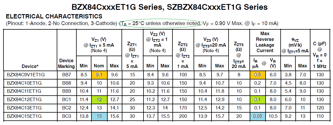
Pumping this into the Excel spreadsheet, at 95C the zener leaks 14.08uA and at 115C it leaks 56.32uA with 8V across the 12V zener if we assume the "BASE" of the exponential equation is "2" and not 1.445.
| Zener DATA SHEET DATA | Onsemi | BZX84C12ET1G | |||||
| 0.00060 | uA Leakage 25C From Curve | 0.06000 | uA Leakage HOT From Curve | ||||
| 0.100 | uA Leakage 25C |
10 | uA Leakage Hot |
150 | Temp for
HOT uA Hot = Data Sheet @25C * uA typical Hot / uA typical 25C |
||
| 2.000 | +Log (I_Hot/I_25C ) |
125 | Delta T | 1.445 | Calc'd �Base� for every 10C |
Ileak =
Iref *BASE^(dT/10C) |
|
| 10.00% | Aging | 1.445 | �Base� to use for every 10C |
||||
| Junction Temp C | 25 C | 85 C | 95 C | 105 C | 115 C | 125 C | 150 C |
| Ileak Ratio HOT | 1.0 | 9.1201083936 | 13.1825673856 | 19.0546071796 | 27.54 | 39.8107170553 | 100 |
| Zener Leak Hot + aging | 0.110 | 1.003 | 1.450 | 2.096 | 3.030 | 4.379 | 11.000 |
| uA Zener leakage 25C Base=2 | |||||||
| Junction Temp C | 25 C | 85 C | 95 C | 105 C | 115 C | 125 C | 150 C |
| 0.1 | 0.11 | 7.04 | 14.08 | 28.16 | 56.32 | 112.64 | 637.19 |
| uA Delta to curve | 0.0 | 6.0 | 12.6 | 26.1 | 53.3 | 108.3 | 626.2 |
Safe Operating Area (SOA) is what the power stress the die (the working part of a transistor) can handle with the CASE or AMBIENT of the part held at 25C. With power devices, think "liquid cooling" here to keep the case at 25C.
The ONSEMI MMBT2222A SOT-23 has a generous SOA for a tiny part, so it isn't a lot of fun to discuss. With the ambient held at 25C, we can get 40V * 5.5mA = 220mW which matches its data sheet limits (225mW). For a 1 second pulse (again with the ambient/case magically at 25C), we can get 1100mA * 1.1V = 1.2W or at 40V, 40V * 26mA = 1.04W into it.
For 1 msec, at 20V we can get 0.4A through it at 25C with it mounted on the equivalent of a 1" by 0.75" by 0.062" piece of FR5. What happens at 95C?
Answer: The allowed current drops to keep the junction hot spot temperature below its maximum rated of 150C:
0.4A * (150C-95C) / (150C-25C) = 0.176A
This 176mA is with no derating or margining. With a standard 0.7 derating, this drops down to 0.176*0.7 = 0.123A. That ends up only being 30% of rated.
Just for the fun of it, I thermally abused some parts a few decades ago. They worked after the abuse. So I left them running at a moderate, but allowed, stress level. A bit more than a week later, I had parts fail (shorted.) There was latent damage that took some time to show up.
( Curves from Onsemi.)
12.6V * ( 1 + 10%) / (1.1 A * 0.7 margin) = 18 ohm resistor with the transistor fully saturated.
If the capacitor starts at 30V and the 2N2222 is not fully saturated, we'll have to iterate on the resistor value and the SOA curve to find the correct value. Another choice would be to limit the dV/dt on the capacitor to limit the current flowing from I = C dV/dt through the large cap on the 2N2222.
2. If we want the 2222A to turn off quickly, we have to pull current "OUT" of the base with the drive circuit. A common way to do this is to reverse the polarity of the Vbe junction (but not to the exceed its 5V rating) with the driver.
3. If we want the 2222A to turn off quickly, we have to keep it out of saturation. Enter in the discussions of "BAKER" and "Schottky" clamps. When deciding between a "Schottky" clamp and a PN based Baker clamp, consider that the Schottky adds more capacitance from collector to base than a Baker clamp.

4. When driving a transistor into saturation, Hfe drops a lot. The Hfe drop doesn't become strong occur until the Base to Collector diode is forward biased. To make life easier, design your circuit to accept a Vce sat of 0.25 to 0.3V.


All curves on this page are from Onsemi-Conductor's website.
.
 ( New
2024 index page.)
 _( Old 2003 index page.)
 _( AMP Second index
page.)
 ( Fancy index page.)