Gertrude and Fred Headphone Amp with Legos All Around
A Headphone Amplifier Running from four AA Rechargeable Batteries
Version 0 of the design had too many
warts to warrant sharing it.
Version 1 of the design sounded great!
However, Version 1 doesn't like mismatched batteries on a slow power
down.
Version 1.2 adds a little polish to version 1. Still doesn't like
mismatched batteries.
14 Dec 2025, Web Page Ver 0
Ver. 0 was built and modified
Ver. 1.0 was built and shown below with a LEGO phone support.
Ver. Ver. 1.2 is a minor clean up of Ver. 1.0, but it is not yet built

-
----------------------------------------------------------------------------------
-
I needed a clean driver for my 30 ohm headphones I listen to at work to try to stay sane. The sound right out of the phone 3.5mm jack was "lacking"
Goals:
Be CLASS A up to around 105dBpk (not rms) into the low impedance headphones that I and my friends use.
Run a 5 day 12 hr/day work week (60 hrs) on 4 AA rechargeable batteries ( 2500mA-hr ENELOOP PRO ).
Optimize for 1.2V per battery and "try to work" at 1.0V per battery.
Be easily modified to work from 8 AA batteries (+/- 6V peak, +/- 4.8V nom) for higher impedance headphones. (8 batteries are needed to be 6.6 dB louder)
Behave during minor overdrive (Behave = no oscillations, Servo loops recover without ringing)
Behave if one battery is missing (Behave ~ = 1mW DC out into 30 ohms or 0.17V)
Survive brief battery reversal or at least limit the cost of damaged parts.
Low DC offset. 60dB down from 1mW at 30 ohms is 173uV.
Do nothing nasty with brief clipping (2X past 105 dB). Hey, if you want to listen to square waves that's your choice, just don't expect it to sound good.
Do nothing nasty with a hot plug on the input, that doesn't mean it won't be LOUD
Do nothing nasty with a hot plug on the output. (Version 0 of the headphone amp failed this)
Operate without a metal case (I live near an AM Radio Station transmitter that shows up when I wave my scope probe in the air.)
Be inexpensive enough I don't get in trouble with my spouse ;-}
Room temperature use only (less than 40C in the case). It doesn't have work if left in the car in the summer. I know what 60C feel like. It gets over 60C in the car with a window reflector in place.
I’d like to use something based on the 6W Gertrude and Fred amp I designed 20 years ago.
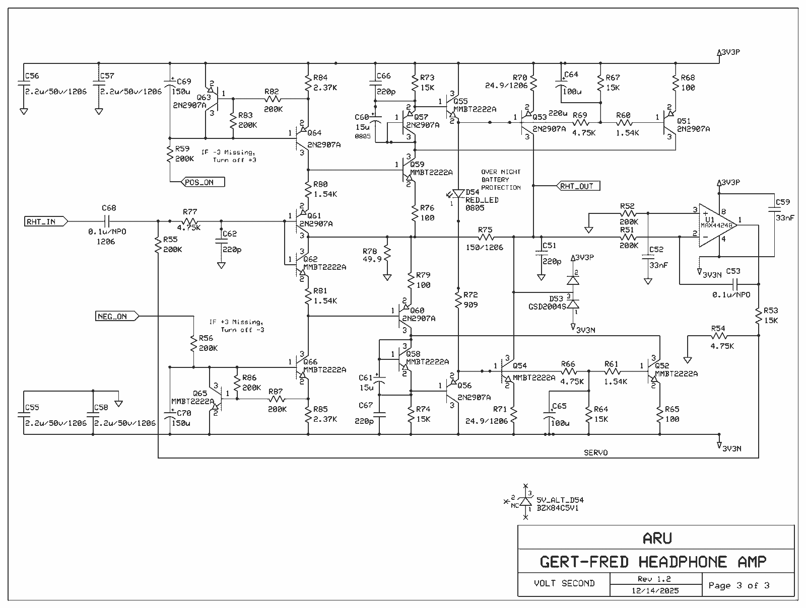
A technician I worked with couldn't keep a 2N2222 (NPN) and an 2N2907 (PNP) straight. He'd called the NPN's Freds because they were "Male" and the PNP's Gertrudes because they were "Female." If I blew up a 2N2222 in testing, I'd ask him to replace the 2N2222 in the driver stage and it would take all day to get done. If I said "Fred's dead in the driver", he'd replace it in minutes.
When he heard I was an audiophile, he said: "Ya know, I think you could design an awesume Audio Amp using nothing but Gertrudes and Freds. It wouldn't have a lot of power, but it would be awesome.”. I designed a good sounding one with 14 2N2222A and 14 2N2907A leaded transistors for the output. The design ran hotter than expected (too hot for my comfort.) I never shared that design. The load is driven from the collectors of the output power devices, it does not work like an emitter follower.
A comparison of the leaded Gertrude and Fred amplifier output packages.
A TO-92 leaded device has an Rth of 200C/W junction to ambient. A "True Gertrude and Fred" only come in this package.
A TO-92 1W (TO-226AE) leaded device has an Rth of 125C/W junction to ambient. A "In the Spirit of Gertrude and Fred" can be found in this package.
A TO-126 leaded device has an Rth of 104C/W junction to ambient.
I'd like to have some ESD protection. At one of the Audio meets, one of the manufactures said they only needed 600V of ESD protection because their RCA land patterns arc'd over at that voltage. Armed with this knowledge, on the inputs and outputs I'm putting a "spark gap." The spark gap is two square lands with the points facing each other to make a spark gap. The math says at 60Hz this should break down at 270pk. However, an article I read that I can't find back had stated for short impulses, the break down voltage rises, 600V could be real. ESD protection is mostly needed on the input jack for when an input cable is connected to the amp and disconnected the phone end. In this condition, the signals will be exposed.
Static pick up (ESD) from the headphones isn't too likely to get past the ground connection at the output connector. On Version 0 and 1.0 I just put a spark gap on the output just because it was there. A spark gap won't protect the output stage. For 15kV 100pF 1500 ohm ESD protection, a diode with an internal resistance less than about 0.4 ohm clamping to the supply rails is needed to protect the output. In version 1.1, I added a BAV299 (D3, D53) for added ESD protection. A MMBD7000L doesn't protect because the internal resistance is too high. Since the modeling says the BAV will protect, I also changed the MMBD7000L in the on/off network 2 to a BAV299 to keep from adding a line item to the Bill of Material (BOM). That was until I found that a RED LED worked even better.
The on/off switch metal tab is floating so if I mount the amp in a metal case, I can prevent a ground loop. Because of this, the frame of the switch has a spark gap to ground.
I used an output DC offset servo because I hate adjusting POTs and with 40+ years of designing and building feedback loops, I think I can make one that will work good enough. By dividing the output of the integrator op-amp by 4, I make the integrator capacitor look 4 times larger. Meaning the 0.1uF NPO behaves like a 0.4uF capacitor and any "unwanted junk" leaking through the op-amp gets reduced by 12 dB. I used an NPO capacitor because Class 1 ceramics sound good, are stable with time, voltage, temperature and they are not piezoelectric. Class 2 ceramics fail all of these points.
I used individual DC bias servos on the two output stages. These bias loops could cause distortion when the output stage is overloaded. I complained about this risk to a friend and he gave this good advice:
Friend: "You don't like that the output stage goes to class B when it is overloaded and won't sound good? And this happens because the amp was driven too hard. Did the amp sound good when it was over driven?"
Me: No. It won't sound as good when it's over driven.
Friend: Can anybody but you tell whether or not it is the bias loop shifting or the over drive causing the bad sound issue?
Me: Probably not. . .
Friend: So shut up about it and get a life."
I found that with a sinewave, I could get almost 4 times peak output current as the bias current out before the bias distortion was unacceptable. If I needed 45mA peak out (200 ohm feedback resistor in parallel with headphone), I could get by with 11.3mA of output bias. In many headphones, 45mA peak current is deafeningly loud.
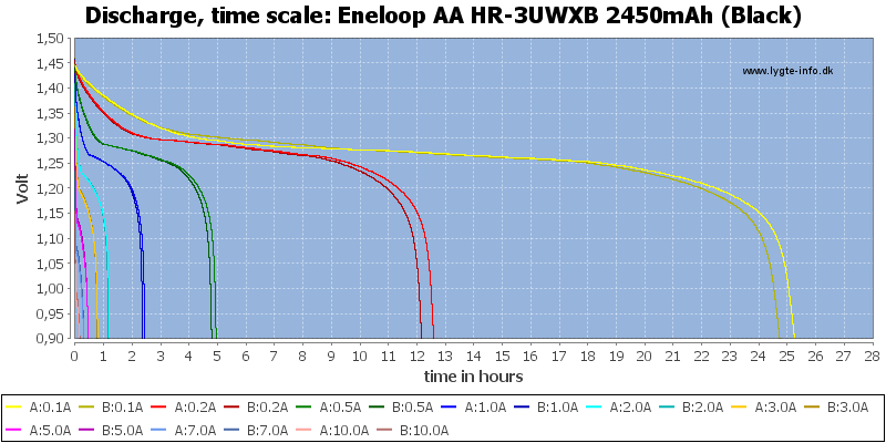
With 33.4mA bias current from the 8AA version and five 12-hour days of use, this was 2004mA hours. This meets the 2500mAh capability of the ENELOOP Pro battery. The Chart below is from this linked website. The ENELOOP Pro Discharge Curves shows the ENELOOP PRO battery can actually produce advertised performance . Look at top yellow 100mA curve and multiply the time by 3 to get the hours of use with the headphone amp V1.1. The ENELOOP 101 site published similar performance. Note that there is not a lot of difference in cutting out at 1.1V vs 1.0V.
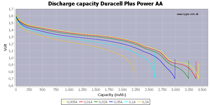
From Duracell Plus Power Discharge Curve is from Lygte-info.dk we see 2625 mAh at 50mA discharge is available from an alkaline battery when the load works down to 1.0V per cell. I typically would use an Energizer AA cell. They may cost a bit more because you can't buy them in bulk at Costco, but I'm always getting "leaker" batteries when I use the Duracells. Taking the batteries out at the end of every use is stupid. Who stores an emergency flashlight or radio with no batteries in it?
E. Minor Changes / Fixes:
I added notes for using this with 8 AA cells (+/- 5V) instead of 4AA cells (+/- 2.5V). I removed the notes for using this at +/- 9V because the output transistors could overheat during power up. This required a "pad" change so I could put an 0805 LED or a SOT-23 at the same spot on the board.
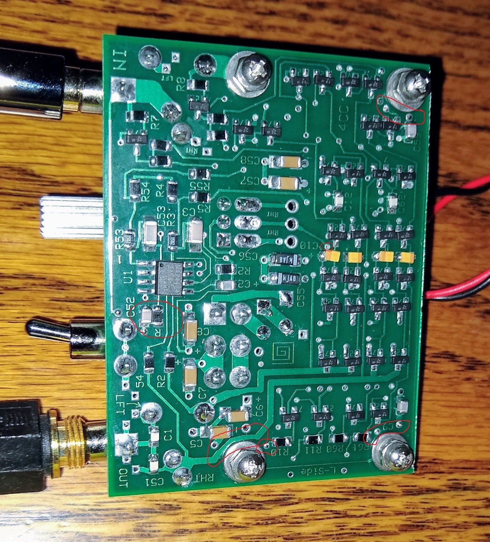
I added D3/D53 for ESD protection on the outputs. I'm depending on the spark gaps for protection on the input (don't conformal coat them!) This doesn't change the topology so I'm not considering this a spin on the version of the amp. I just had to remove some "Gee Wiz" marking on the bottom of the board to fit the two parts (The spiral in the middle and the RHT on the bottom edge).
I corrected the markings of R1 and R51 on the bottom of the PWB (They were marked R2 and 53)
I moved R52 and C52 a little further apart
I moved the bottom Right Output trace a little further from the #2 mounting post. I had to shave 5 mils off the width to make this happen.
I added extra copper under the output transistors to try to get slightly better thermal performance.
I decreased the current in the BLUE LED to 2.37K because with a 1.57K bias resistor, it was too bright.
I'm changing C19, C20, C69, C70 from 68uF to 150uF to reduce the turn on stress during multiple power switching events.
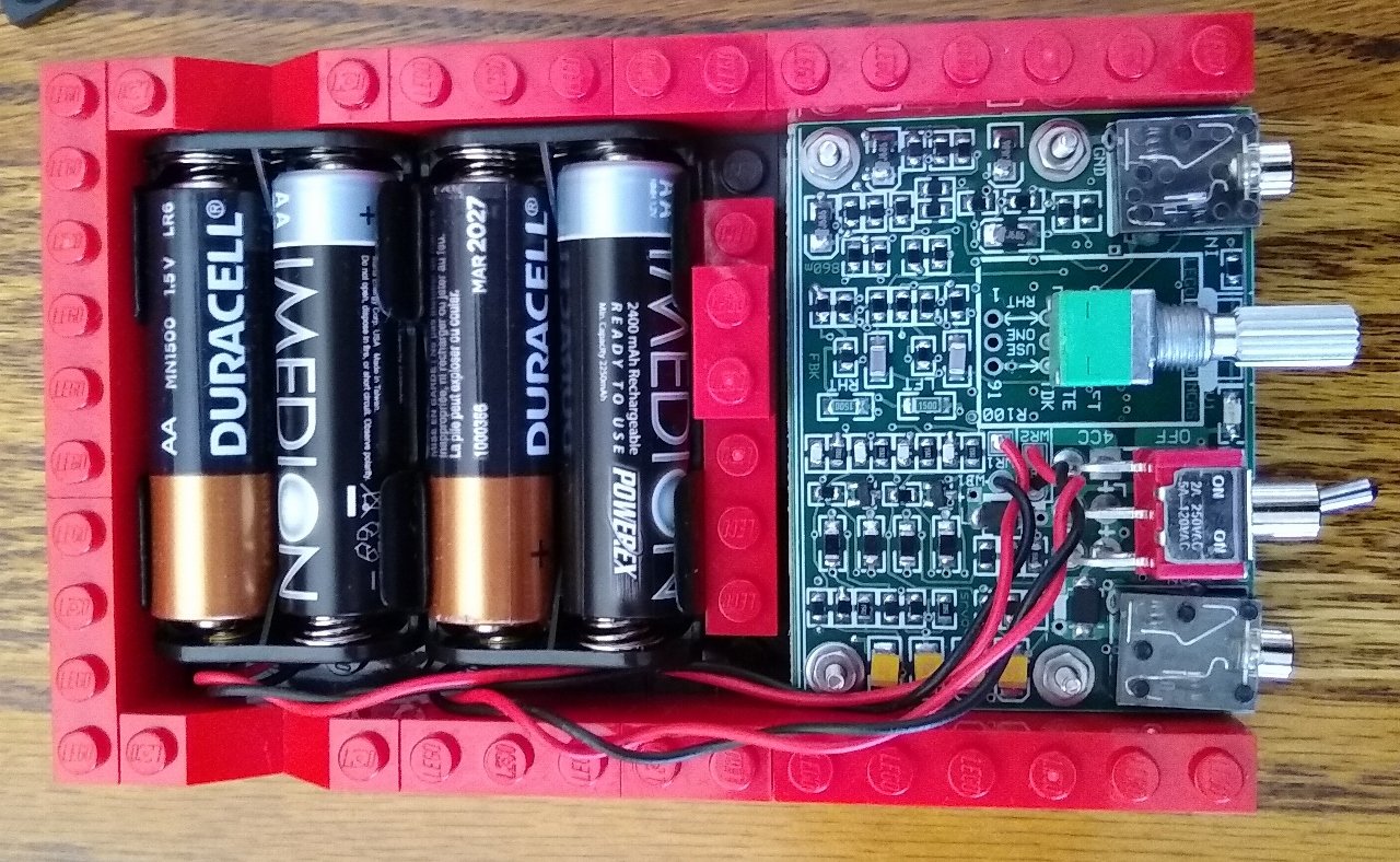
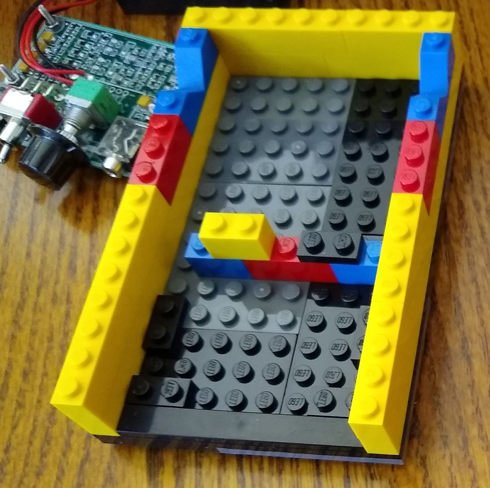
Version 1.0 in an open Lego Case.
Version 1.0 (2nd build) Bottom
I've learned that on hand soldered designs, it is often better to leave a slightly ugly solder joint alone because the thermal stress from cleaning it up can cause damage to the part, particularly if the part is a SMT ceramic capacitor. The solder joints above look better in real life than they do in the picture.
With the iron cold, switch to a narrow solder tip (not a needle point) and then warm the iron up.
Put a drop of liquid flux on the board,
Put a small solder ball on one land. I use a corner on an SO-8 package, pin 3 on a SOT-23.
Add more liquid flux
Hold the part in place with my fingernail and just barely reflow the solder ball. As soon as the solder flows, I remove the iron.
Solder the other parts pin's, do this quickly after the first reflow if it is a SMT cap.
Add more solder to or reflow the first "solder ball joint" if needed.
Gently clean the part with 90% IPA-
NOTE: D4 is 5.1V not 4.3V for 8 battery (5V) use.

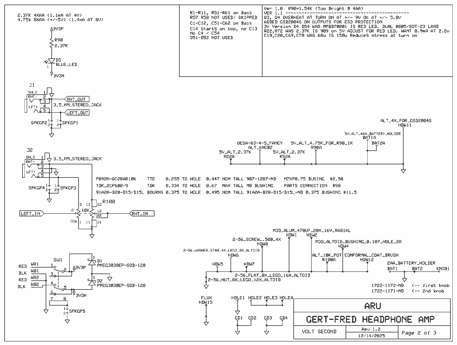
Using the LTSPICE model and looking for ways to bread the amplifier, I found that with +/- 9V rails, the output transistors would be over-stressed for about one second if the power switch was quickly switched on and off back to on. I decided to change notes in schematic for use with 8 total AA batteries (+/- 5V rails).
For use with +/- 5V rails:
D4/D54 becomes a BZX84C5V1 (with data sheet limits at 1mA bias.) (was a RED LED.)
R22/R72 become 2.37K resistors (3.01K will also work, but 2.57K is already on the parts list.) (was 909 ohms)
R90 (the LED bias resistor) becomes 4.75K (was 2.37K)
The battery holders become 4 AA cell holders (instead of two AA)
Changes V1.0 to V1.2 for the 2.5V (3V) version only
Changed D4/D54 from MMBD7000L to an 0805 RED LED. I made the land for this part on the board so it would take a hand soldered SOT-23 or the 0805.
R22/R72 became 909 ohms to give correct bias current with the RED LED.
Changes to both the 2.5V (3V) and 5V version.
Added D3 and D53 on the outputs for ESD protection. You'll need this part or a BAS299 that has a low internal resistance. Not an MMBD7000L (still my favorite SMT small signal diode.)
Changed C19, 20, C69, C70 from 68uF to 150uF for lower turn on stress when the power switch is turned off and back on quickly (seconds apart.) These fit on the same lands as before.
Moved a couple vias further from the screw holes to prevent shorting
Moved the red inner layer 25 mils further from the cut line (to split the ExpressPCB in half) to reduce risk of short.
Moved the right output trace a bit further from the middle screw hole
Corrected marking on bottom for R1 R51
Moved R52 and C52 a bit further apart.
Remember to wear a static strap and work on an ESD safe surface when soldering. If needed, you can spray your normal work surface with "Staticide" before you start working.
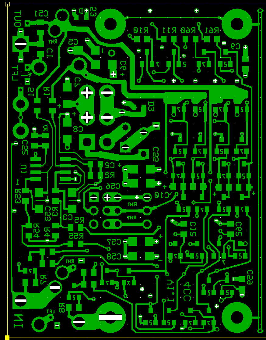
The Bottom Semiconductors are shown above.
The 2N2222s have a "2" next to them
The 2N2907 have a "7" next to them.
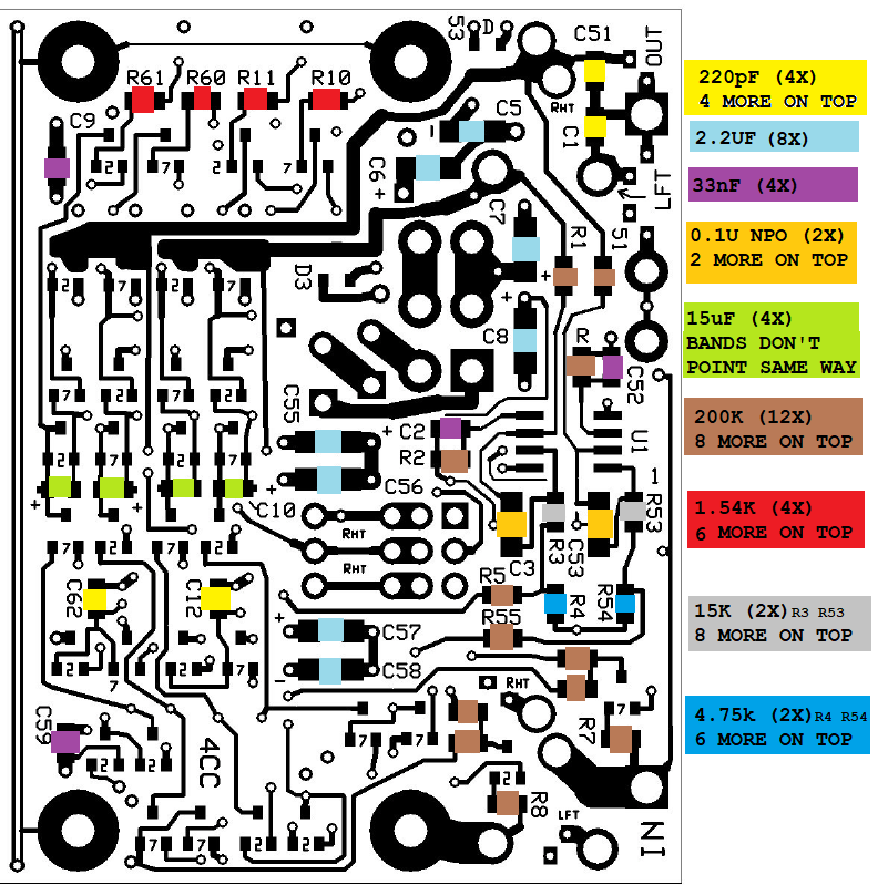
After populating the bottom side, populate the top side. I'd start with the SMT resistors first.

| Qty | Name | Order | Part_ID |
| 8 | 220p | 399-6938-1-ND | C1,C12,C16,C17,C51,C62,C66,C67 |
| 4 | 15u | 478-13512-1-ND | C10,C11,C60,C61 |
| 4 | 100u | 478-13510-1-ND | C14,C15,C64,C65 |
| 4 | 0.1u/NPO | 445-6984-1-ND | C18,C3,C53,C68 |
| 4 | 150u | 478-13157-1-ND | C19,C20,C69,C70 |
| 4 | 33nF | 445-175692-1-ND | C2,C52,C59,C9 |
| 8 | 2.2u/50v/1206 | 399-7019-1-ND | C5,C55,C56,C57,C58,C6,C7,C8 |
| 2 | PMEG3030EP-SOD-128 | 1727-5324-1-ND | D1,D2 |
| 2 | GSD2004S | 112-GSD2004S-HE3_A-08CT-ND | D3,D53 |
| 2 | RED_LED | 732-4985-1-ND | D4,D54 |
| 1 | BLUE_LED | 732-4989-1-ND | D5 |
| 2 | 3.5_MM_STEREO_JACK | SC2405-ND | J1,J2 |
| 17 | 2N2907A | MMBT2907ALT1GOSCT-ND | Q1,Q10,Q11,Q13,Q14,Q17,Q3,Q51,Q53,Q56,Q57,Q6,Q60,Q61,Q63,Q64,Q7 |
| 17 | MMBT2222A | MMBT2222A-FDICT-ND | Q12,Q15,Q16,Q18,Q2,Q4,Q5,Q52,Q54,Q55,Q58,Q59,Q62,Q65,Q66,Q8,Q9 |
| 20 | 200K | 541-200KCCT-ND | R1,R2,R32,R33,R36,R37,R5,R51,R52,R55,R56,R59,R6,R7,R8,R82,R83,R86,R87,R9 |
| 8 | 1.54K | 541-1.54KCCT-ND | R10,R11,R30,R31,R60,R61,R80,R81 |
| 1 | 10K | 91A2A-B28-D15/D15L-ND | R100 |
| 10 | 15K | 541-15.0KCCT-ND | R14,R17,R23,R24,R3,R53,R64,R67,R73,R74 |
| 8 | 100 | 541-100CCT-ND | R15,R18,R26,R29,R65,R68,R76,R79 |
| 8 | 4.75K | 541-4.75KCCT-ND | R16,R19,R27,R4,R54,R66,R69,R77 |
| 4 | 24.9/1206 | 541-24.9FCT-ND | R20,R21,R70,R71 |
| 2 | 909 | 541-909CCT-ND | R22,R72 |
| 2 | 150/1206 | TNP150ACCT-ND | R25,R75 |
| 2 | 49.9 | 541-49.9CCT-ND | R28,R78 |
| 5 | 2.37K | 541-2.37KCCT-ND | R34,R35,R84,R85,R90 |
| 1 | 100DP1T2B4M6QE | EG2404-ND | SW1 |
| 1 | MAX44248 | MAX44248ASA+TCT-ND | U1 |
| 2 | 2AA_BATTERY_HOLDER | 377-1559-ND | BAT1,BAT2 |
| 1 | KNOB_FLUTED_W/SKIRT _0.250"_PLAST | 1722-1191-ND | KNOB1 |
Below are the different parts you'll
need if you want to make the 5V version (8 AA cells).
| Qty | Name | Order | Part_ID |
| 2 | BZX84C5V1 | BZX84C5V1-E3-18GICT-ND | 5V_ALT_D4,5V_ALT_D54 |
| 2 | 5V_ALT_4AA_BATTERY_HOLDER | 377-1560-ND | BAT1A,BAT2A |
| 2 | 5V_ALT_2.37K | 541-2.37KCCT-ND | R22A,R52A |
| 1 | 5V_ALT_4.75K_FOR_R90_1X | 541-4.75KCCT-ND | R90A |
If ordering the 5V parts, don't order the
LEDs for D4, D54,
The two AA cell battery holders,
The two 909 ohms for R22, R52
Order one less 2.37K for R90 (Blue LED brightness)
Optional Sundries
| Qty | Name | Order | Part_ID |
| 1 | CONFORMAL_COAT_BRUSH | 473-1391-ND | HDW12 |
| 1 | FLUX_LIQUID_RMA_IPA_CLEAN | 315-CQ9LF-1.0-ND | HDW15 |
| 1 | MOD_ALTOID_BUSHING_0.187_HOLE_2X | 36-730-ND | HDW4 |
| 1 | 2-56_NUT_8X_LEGO_12X_ALTOID | H723-ND | HDW5 |
| 1 | 2-56_WASHER_STAR_4X_LEGO_8X_ALTOID | H728-ND | HDW6 |
| 1 | 2-56_FLAT_8X_LEGO_16X_ALTOID | H733-ND | HDW7 |
| 1 | 2-56_SCREW_.500_4X | H701-ND | HDW8 |
Alternate Parts
| 1 | OESA-63-4-5_FANCY | 226-4149-ND | ALT_KNOB2 |
| 1 | ALT_4X_FOR_GSD2004S | 4786-BAS299CT-ND | HDW11 |
| 1 | ALT_10K_POT | 987-1287-ND | R100A |
Purchase your parts from a place that has quality control over their parts like Digikey, Mouser etc. I've heard complaints about parts coming from Ebay etc.
You will also want liquid flux (water-soluble), an "acid brush", a pint of 70% Isopropyl Alcohol, a solvent dispenser and a bottle/can of conformal coating (self extinguishing).
I prefer to use "leaded" solder. It will never grow tin whiskers. I still haven't seen proof that lead free RoHS solder is whisker free when the time duration is measured in decades instead of 90 day warranties. Conformal coat will not stop tin whisker growth, but it does reduce the risk..
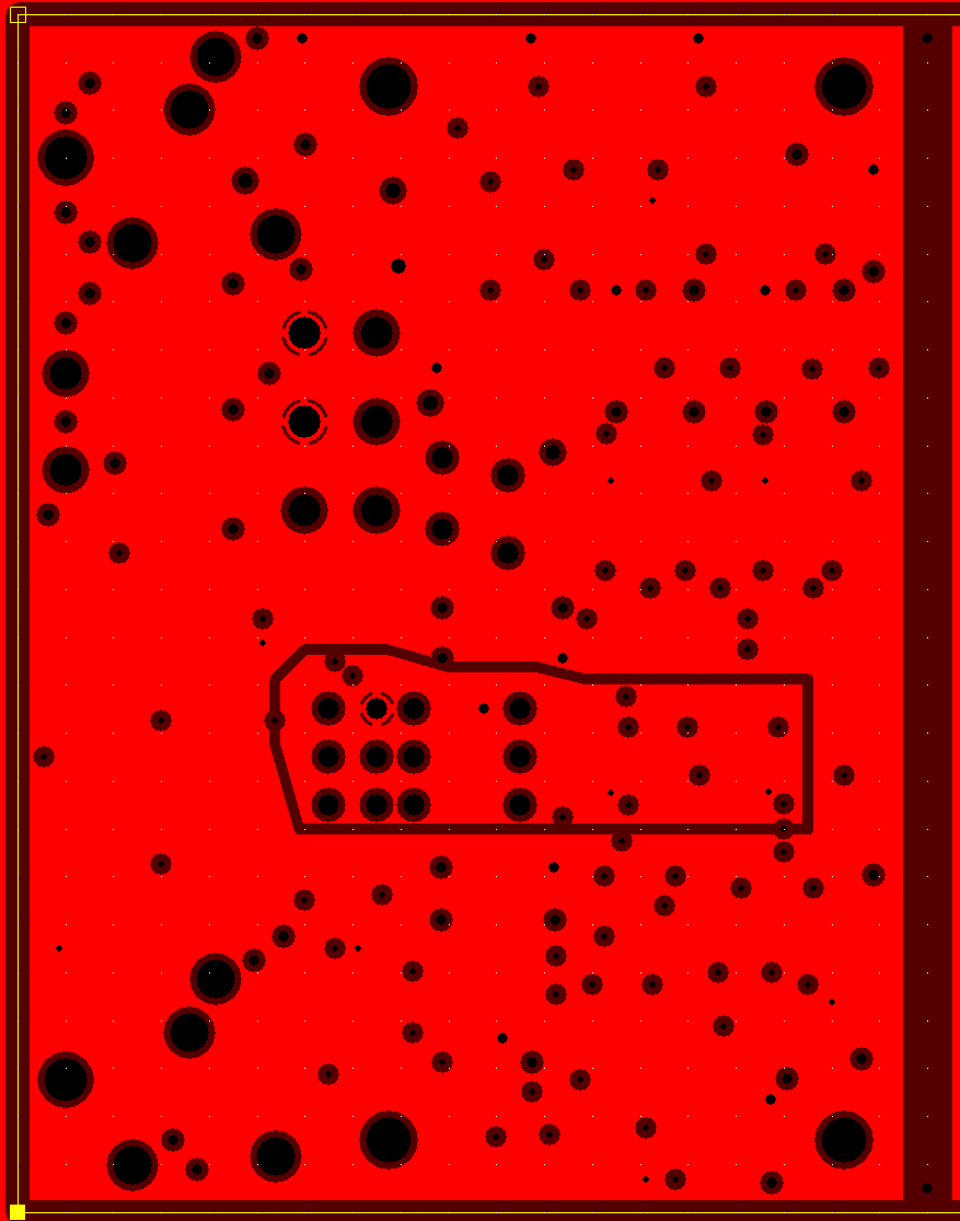
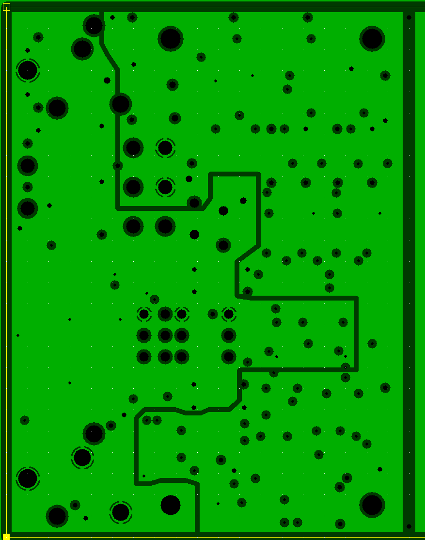
The section is on the Printed Wiring Board Layout and related notes. For analog/ power cards, I prefer most traces to be wider than 10 mils and I prefer 20 mil via diameters versus the smallest ones available. A 20 mil via has an aspect ratio of 3:1 on a 62 mil board. An aspect ratio of 3 is reasonably strong. Vias in the PWB will need a wider trace (or teardrop) attaching to them where they connect to 15 mil or thinner traces.
The finished 2.5" by 3.8" EXPRESS PCB board surface is not full. This allows you to either make copies of this circuit on the board and/or add another circuit to the board.
MINOR LAST MINUTE CHANGES ARE NOT SHOWN
To cut the board in half, I normally tape the board surface with Blue Painter's tape and with a metal ruler as a guide, I score the top and bottom 2 dozen times with a sharp box cutter to break the board sections apart. If it is not an "easy" snap to make, score it more times. Wear gloves so you don't cut yourself and don't score the board on top of something your "significant other" will be pissed at you if you scratch it up or cut it up.
Yes, I put a smiley face on the PWB. In a low output voltage ripple switching power supply I designed, I had to place cuts in the ground planes around the filter capacitors to get the output ripple into spec. Unintentionally it made a "smiley face" in the bare PWB. I got in mild trouble for it, but strangely, without the happy face, the design didn't work as well. So now on my "fun" projects and on test equipment, I put a "smiley face" or something like that on the board.
-
The output stage must clip (voltage or current) before the stage before it. That stage must clip before the stage before and so-forth. If the first stage bias clips, it's softstart capacitor will pickup an imbalance an the output voltage and bias points will not settle quickly (it will sound noticeably bad after the clipping stops.)
At 2.1V on the battery, we have about 3.3 diode drops (0.62V/diode) to use for gain. Except for the output stage, which we'll allow to saturate, we'll want to keep the collector to emitter voltage greater than the base to emitter voltage (in magnitude.)
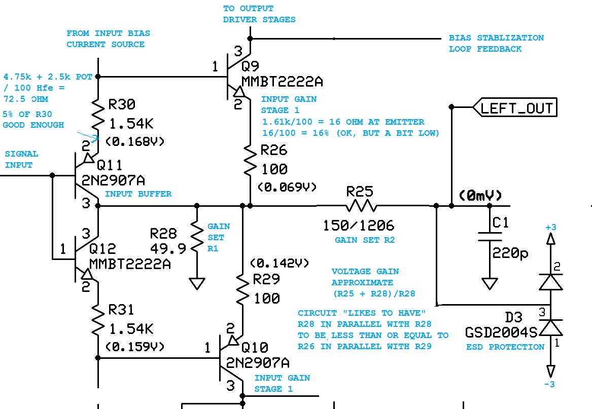
We'll set the first stage current source up with about 0.3V in the emitter instead of 0.6V. Discrete transistors can have 26mV mismatch in Vbe between part that can reach 50mV of mismatch in very conservative uses. Having 11 times this voltage in the emitter degeneration resistor helps reduce variation between unit. The two resistors needed to do this (R32/R33) also help to implement the “don't damage the headphones if a battery is missing function.” This input bias current source takes up just under 1.5 diode drops of our voltage margin.
On the input buffer first gain stage, we will allow the voltage drop in the emitter resistor to drop further. Normally the voltage drop in R26 would be assumed to be the same as in R30, but because Q9 conducts more current, its Vbe voltage drop is higher than Q11. If I double the value of R26 and R30 to make this "look better", I'll loose loop gain and the output impedance will rise. I'd rather have the lower output impedance than the higher voltage drop in R26.
This set up gives me 1.3 diode drops of voltage for a total of 2.8 diode drops out of 3.3 diode drops available to make music. This leaves 0.5 diode drops (0.31Vpk) of input voltage in "ideal operation" and a bit more than twice that input voltage in the "Yep, it still works operation" range.
(150+50 ohm feedback in parallel with 30 ohm load) = 26 ohms effective load
(2.1V rails - 0.2V Vbe sat output stage) * 26 ohm / (26 ohm + 24.7 bias set) = 0.975V peak output possible into 30 ohm at a near dead battery
0.975V / 4 gain = 0.244V pk input will saturate the output with a near dead battery.
The input stage is in "ideal operation" to about 0.31Vpk so we have 0.31-0.244V = 66mV of margin (twice the calculated bias voltage on R26) it all works out. We'll lose available "clean" output swing if we double both R20 and R26 values (and R31 and R29). If we were running from +/- 12V rails, I'd bias this front end up with more current and higher voltage drops.
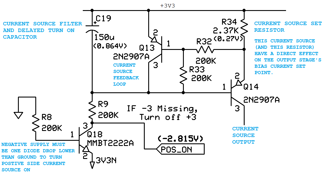
The output stage generates a lot of current gain (more than 10K
times.) A DC bias feedback to stabilize the bias current point. A
current driven output is also more stable into a capacitive load and
is less likely to have RF stability issues. This output stage needed
to have the RF gain rolled off by C16. C10 provides a bonus because it
allows the feedback current from Q1 to pull (push?) the base of Q5
above the voltage rail to completely turn Q3 off.
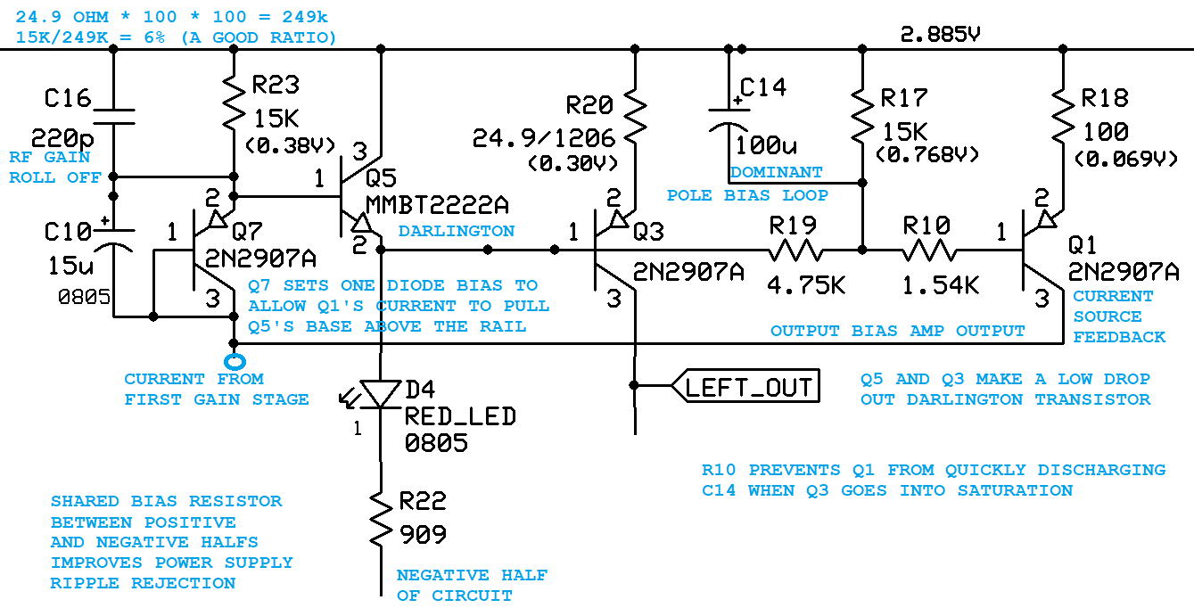
The transistor's current gain (Hfe) can vary from 100 to 300. On a separate model I varied the Hfe of the 2N2907A and 2N2222A 3:1. All like transistors varied the same way at the same time, meaning all 2N2222A at high gain at same time, but the 2N2907A could be at a different gain. When I did this the output impedance did not significantly change. The output bias current changed only 2%.
The output bias point is generated from a multiple of the Vbe of a transistor that generated the input bias current. As the board heats up, this input bias current drops and thus the output bias current drops. Changing the temperature from 15C to 45C changed the output bias current by 1.34:1. This was expected.
417uA for the Power LED (0.83mA total)
130uA for the DC offset opamp per amp
25uA DC cancellation bias resistors at 0.5V at op-amp out
11.2uA for missing battery protection
105.6uA first stage bias
972.8uA second stage bias
835uA third stage bias with LED
11.9mA Output stage bias
14.4mA total (nominal per channel) 28.8mA total
Use NPO caps so that distortion and microphonics don't get into sound path.
Place the DC servo out to be more than 6dB down at 20 Hz to avoid clipping with 2.2V rails
Want settling time between 0.5 and 2 seconds. Slow means less interaction with the "music" but more stress during turn on.
Want rail to rail out from DC servo to be able to correct for 1% part variations on one end
I don't want the servo to have full control of output
The MAX44248 ($2.50) works down to 2.7V and draws 0.26mA of bias current with nearly rail to rail inputs allowed. The input offset current is 600pA with a 7.5uV offset voltage. The input works to 1.5V of the rail for common mode. (1V typical.) This says any input bias resistor over 7.5uV/600pA = 12.5K will degrade the offset voltage. But we don't need 7uV of offset voltage. My target headphone is the ATHM50 which requires 550mVpeak for 105 dB. Let use 0.1% of that for the allowed offset or 0.55mV (8nW into 38ohms). 0.55mV/600pA gives 916K total for the input bias resistors on the amp or 458K each. I'm balancing the inputs even thought it isn't needed with this amp just so I can change op=amps if needed
As a potential alternate, the LT6012I ($4.60) is 75uV offset with 500pA of offset current.
The following article discusses DC offset and DC op-amp bias issues in detail: “https://www.edn.com/op-amp-dc-error-characteristics-and-the-effect-on-high-precision-applications/ “
High lights from the article are as follows:
IB = (Ibpos + Ibneg)/2 Voffset_IB = IB * (Rpos - Rneg)
Ios = (Ibpos - Ibneg) Voffset_Ios = - Ios * (Rpos + Rneg) /2
Solve for Ibneg:
Ios == (Ibpos - Ibneg)
Ibpos = Ios + Ibneg
IB == (Ibpos + Ibneg)/2
2* IB = Ibpos + Ibneg ( + current is flowing into opamp per Maxim)
Combine the two
2*IB = Ios + Ibneg + Ibneg = Ios + 2*Ibneg
2*IB - Ios = 2*Ibneg
Ibneg = Ib - Ios/2
Ibpos = Ios + Ibneg = Ios + Ib - Ios/2
= Ib + Ios/2
Vos_bias = - Ibpos * Rpos - (- Ibneg * Rneg) (Current is “into + and -” inputs.)
= Ibneg * Rneg - Ibpos * Rpos
= (Ib - Ios/2) * Rneg - (Ib + Ios/2) * Rpos
= Ib * (Rneg - Rpos) - Ios * (Rneg + Rpos)/2
7.5uV DC offset MAX44248ASA
300pA DC bias 300pA * 200k = 60uV if + input R is low impedance.
600pA DC offset 600pA * 200K *2 = 240uV if + input R matches the “-” input R.
| Vos mV op-amp |
Ib | Ios | Units | Rpos | Rneg | mV IB | mV Ios | Total mV | |
| MAX44248 | 0.0075 | 300.0 | 600.0 | 1.00E-012 | 202,000 | 199,999 | 0.0006 | -0.121 | 0.1287 |
| MAX44248 | 0.0075 | 0.0 | 600.0 | 1.00E-012 | 202,000 | 199,999 | 0.0000 | -0.121 | 0.1281 |
| MAX44248 | 0.0075 | 300.0 | 0.0 | 1.00E-012 | 202,000 | 199,999 | 0.0006 | 0.000 | 0.0081 |
| MAX44248 Nom |
0.0020 | 150.0 | 300.0 | 1.00E-012 | 202,000 | 199,999 | 0.0003 | -0.060 | 0.0626 |
| MAX44248 | 0.0075 | 300.0 | 600.0 | 1.00E-012 | 202,000 | 4,749 | 0.0592 | -0.062 | 0.1287 |
| MAX44248 | 0.0075 | 0.0 | 600.0 | 1.00E-012 | 202,000 | 4,749 | 0.0000 | -0.062 | 0.0695 |
| MAX44248 | 0.0075 | 300.0 | 0.0 | 1.00E-012 | 202,000 | 4,749 | 0.0592 | 0.000 | 0.0667 |
| MAX44248 Nom |
0.0020 | 150.0 | 300.0 | 1.00E-012 | 202,000 | 4,749 | 0.0296 | -0.031 | 0.0626 |
| LT6011 (non-A) | 0.0750 | 900.0 | 900.0 | 1.00E-012 | 202,000 | 199,999 | 0.0018 | -0.181 | 0.2577 |
| LT6011 (non-A) | 0.0075 | 0.0 | 900.0 | 1.00E-012 | 202,000 | 199,999 | 0.0000 | -0.181 | 0.1884 |
| LT6011 (non-A) | 0.0075 | 900.0 | 0.0 | 1.00E-012 | 202,000 | 199,999 | 0.0018 | 0.000 | 0.0093 |
| LT6011 (non-A) | 0.0750 | 900.0 | 900.0 | 1.00E-012 | 202,000 | 4,749 | 0.1775 | -0.093 | 0.3456 |
| LT6011 (non-A) | 0.0075 | 0.0 | 900.0 | 1.00E-012 | 202,000 | 4,749 | 0.0000 | -0.093 | 0.1005 |
| LT6011 (non-A) | 0.0075 | 900.0 | 0.0 | 1.00E-012 | 202,000 | 4,749 | 0.1775 | 0.000 | 0.1850 |
Series protection is out of the question for we can't afford 0.3 to 0.4V for a schottky when running from two AA batteries per supply rail. There aren't suitable MOSFETs to use for active series protection with just 2V to run the circuit..
The impedance of the ENELOOP PRO batteries is listed as 0.05 ohm each (0.10 ohm total)
1 foot leads of #26 to the battery is 40.8mohm + 50 mohm 2X NiMH battery = 91mohm. Estimate 0.010 ohm per contact to battery for 0.13 ohm. If using Energizer alkaline batteries, the internal resistance raise to 0.15 ohm per battery or 0.38 ohms.
With 3.0V total unloaded from the ENELOOP cells, this is 23 amps. This is enough to fry a 0.080" wide 1 oz copper trace in 0.38 seconds (per Onderdonk) Without adding extra protection, protecting against reverse battery isn't going to happen. However, when testing with a bench supply, it is easy to get leads swapped. With a 1A current limit on the bench supply, we can handle this for 50 seconds (a long time to be going "Duh, why ain't it working").
If we want a bit more protection and are willing to accept more voltage drop in the battery line, the Littlefuse resettable fuses are an option. 0805L020 Would limit the current to 3.8A (Switch rating). But it would add cross talk between left and right.
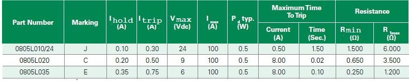
I'd rather not have the extra series resistance in the supply rail. It only should be about 40mV of voltage drop, but in the 80s I had problems with these devices with ambient temperature and have lost a little faith in them. The trade-off I I'll take here is to prevent issues during lab testing and have a beefy anti-parallel diode to protect the parts and caps.
The REF-DES in LTSPICE do not match the REF-DES on the PBA.
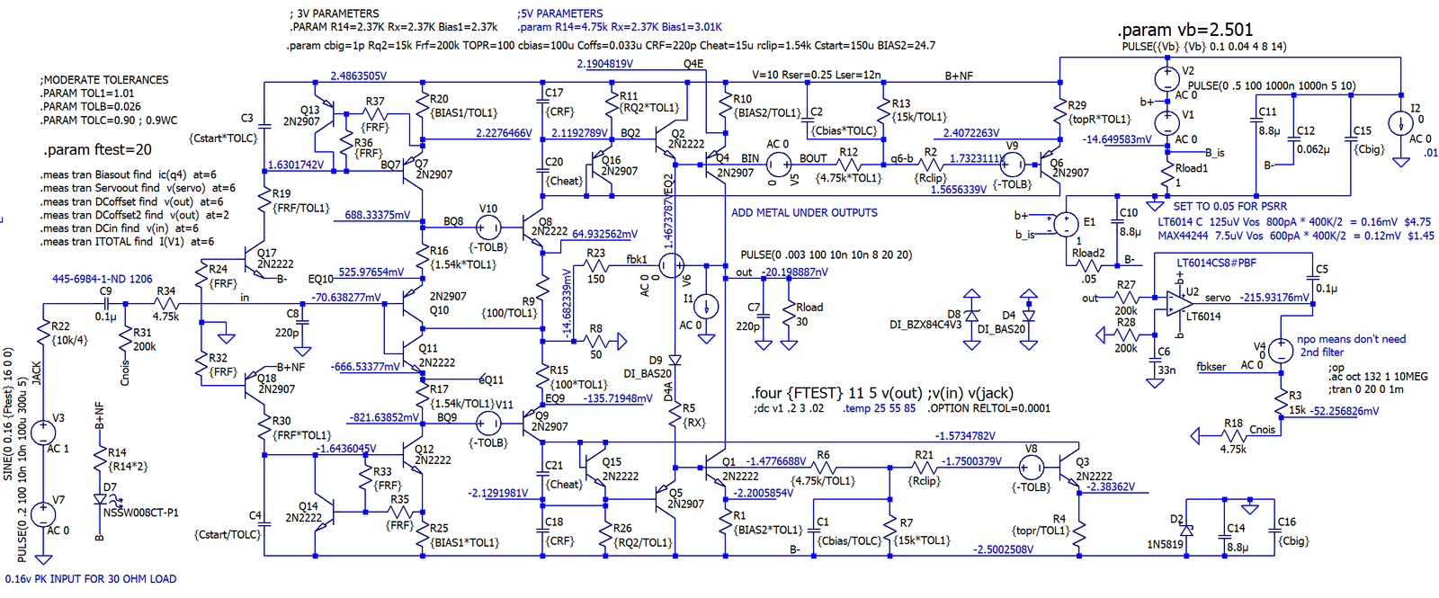
The frequency response is fairly flat. I didn't feel the need to flatten the < 1dB rise just above 10Hz.
R22 on PBA or R5 in LTSPICE was 2.37K (RX) in these runs. I found out at the last minute the odd harmonics are lower with 1.57K for this resistor.
The frequency peak at ~14 Hz is from an interaction with the DC Servo loop. If you want the peak lower, reduce R28 (in LTSPICE) from 4.75K to 2.37K. The down side of doing this is that this will reduce the amount of DC offset the servo can control (a risk) for the benefit of reducing the size of the low frequency peak (may or may not be a good thing). I’m leaving it at 4.75K for my use.
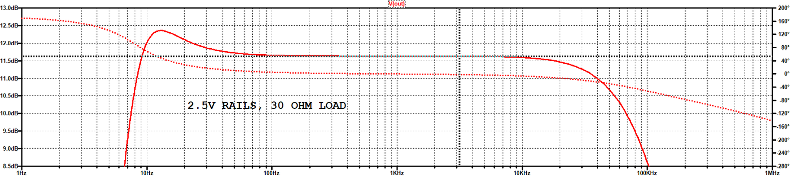
This design has a fairly flat output impedance a bit less than 1 ohm. The design actually needs a little bit of capacitance (220pF) on the output for stability. The 220pF (CRF, C17 above) is because without it, the amp was picking up a nearby AM radio station and you could hear it in the output.
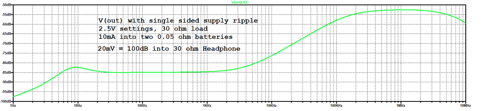
The expected load current is 10mA and the ENELOOP battery is supposed to have a 0.05 ohm internal resistance per battery. The power supply induced cross talk should be as follows with single ended noise:
(These runs MAY have been affected by changing "RX" from 2.37K to 1.54K.)
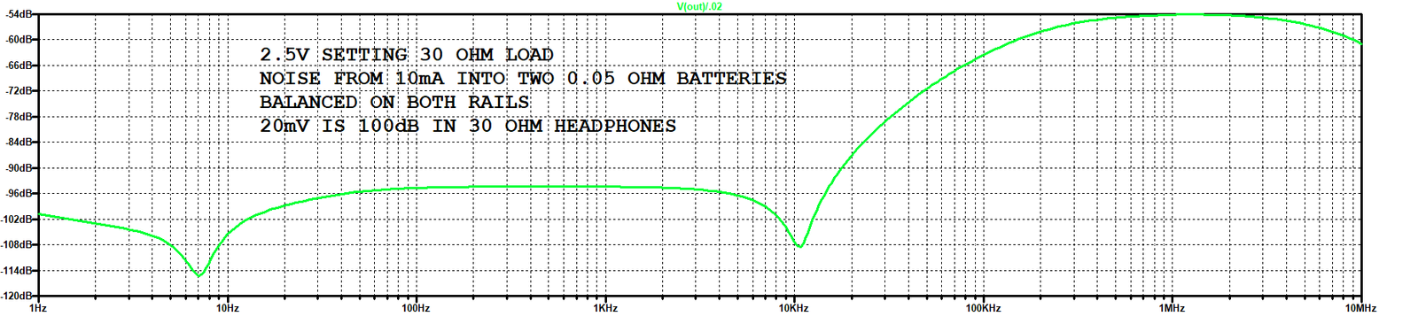
With balanced supply rail noise (same ripple on +2.5 as -2.5) it looks better.
Below we have the fast turn on and slow turn off response with a 2nd fast turn on included. The sinewave is turned on at 16 seconds and is set to demand full class A power from the amp. The turn off bump is 202mV peak, so we miss our 1mW goal of 173mV by just a little bit.
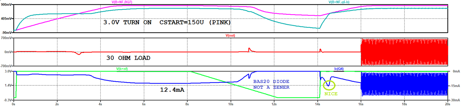
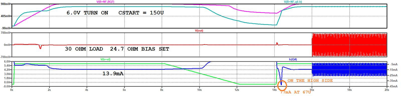
Below is the 6V turn on. Cbias1 at 150uF makes the first turn on spike larger (-230mV for 150msec), but the 150uF greatly reduces the turn on over current seen in the output stage Ic(Q4) at 14.3 seconds. This run is with "Moderate" tolerances picked in the parameter statements. With "Small tolerances", the spike drops to -150mV. These turn on /turn off voltage bumps are still "small" when compared to full Class A output power occurring at 18 seconds.
The part tolerance settings used were as follows:
;MODERATE TOLERANCES
;SMALL TOLERANCES
.PARAM TOL1=1.01
.PARAM
TOL1=1.001
; 1% resistor is usually 2% over temperature and aging
.PARAM TOLB=0.026
.PARAM TOLB=0.0125
; nKT/q is normally 26mV twice this is very
worst case
for
part
to model/datasheet matching
;1X nKT/q is more likely to be seen as an
edge condition
.PARAM TOLC=0.90 ; 0.9WC
.PARAM TOLC=0.98 ; 0.9WC ; Buy 10% caps
and assume they track reasonably well
over age and temperature.
Note: With 13.9 mA bias in Q4 and (6V
- 0.34V emitter) we get 78.7mW of power loss. With heavy copper n the
board, the board will conduct heat well and we should see 357C/W
thermal performance. this results in a 28C rise over ambient or
58C with a 30C ambient. This is acceptable.
This distortion data is close to full "Class A" output power:
643mVpk^2/30 ohm/2=6.8mW into 30 ohms or +8 dBmW from a 2.5V
run.
The output bias is 12.05mA
The total rail current is 14.6mA * 2 = 29.28mA ( RX = 2.37K )
30mA * 12hr/day * 5 days = 1800mAh from battery (2500mAh available)
This 30 ohm test load is driven to almost where the amp leaves the Class A bias point at 20 Hz.
Harmonic
Frequency
Fourier Normalized
Number [Hz]
Component Component
1
2.000e+01 6.433e-01
1.000e+00 (21mApk output)
2
4.000e+01 3.190e-04 4.959e-04
3
6.000e+01 4.303e-04 6.689e-04
20Log6.69e-4=-63dB
4
8.000e+01 1.023e-04 1.590e-04
5
1.000e+02 9.415e-05 1.464e-04
6
1.200e+02 3.155e-05 4.904e-05
7
1.400e+02 2.286e-05 3.553e-05
8
1.600e+02 8.362e-06 1.300e-05
9
1.800e+02 4.829e-06 7.507e-06
10
2.000e+02 1.521e-06 2.365e-06
11
2.200e+02 6.151e-07 9.562e-07
Total Harmonic Distortion: 0.086254%(0.086256%)
For this run the measurements we got were:
biasout:
ic(q4)
= -0.0120488 at 6
servoout: v(servo) = -0.215932 at 6
dcoffset: v(out) = -2.01989e-008
at 6
dcoffset2: v(out) = -2.01989e-008 at 2
dcin: v(in)
= -0.0706383 at 6
itotal: i(v1)
= -0.0146496 at 6
This is design abuse. This WILL SHOW DISTORTION that will occur if the design is operated outside the intended power limits. Neither I nor any of my friends I loaned my amp to every played the music loud enough for this to occur in use. This is a similar behavior to a push pull tube amp with separate bias resistors and separate bypass capacitors on the output stage.
To reduce this requires a combination of
1. Raising the bias current so it occurs at a higher power level at the cost of a shorter battery life and possibly needing a larger output transistor or multiple paralleled transistors to handle the power loss.
2. Adding more local feedback and higher voltage drop in the output stage so that a bias pot can be added to the input driver to control the bias point. This is at a cost of a reduced peak output voltage, accepting a higher output impedance (a lower damping factor) and accepting a higher risk of failure if the output stage is shorted.
I would consider slightly raising the bias current, but for the rest of it, I'd take my friend's advice and "shut up about it and get a life"
This model assumes the board is powered up during ESD event. If it is not powered up and the ESD charge all flows into the two 2.2uF ceramics on the power rail, the power rail moves by (use Q = CV ):
15000V * 100pF / 4.4uF = 0.34V
This low of a voltage bump says the ESD results will be similar whether it is powered on. Surviving powered on is usually harder in the real world.
The ESD generator is shown on the bottom of the given schematic. I find it is better to put a 15kV voltage step in bottom of the 100pF ESD diode than trying to charge the 100pF cap up and then use a switch to discharge the capacitor into the circuit. When validating the "switch" SPICE model, the 100pF often fails to deliver 100% of the energy stored in the capacitor. When using a voltage step in series with the 100pF cap, I always get full energy delivered.
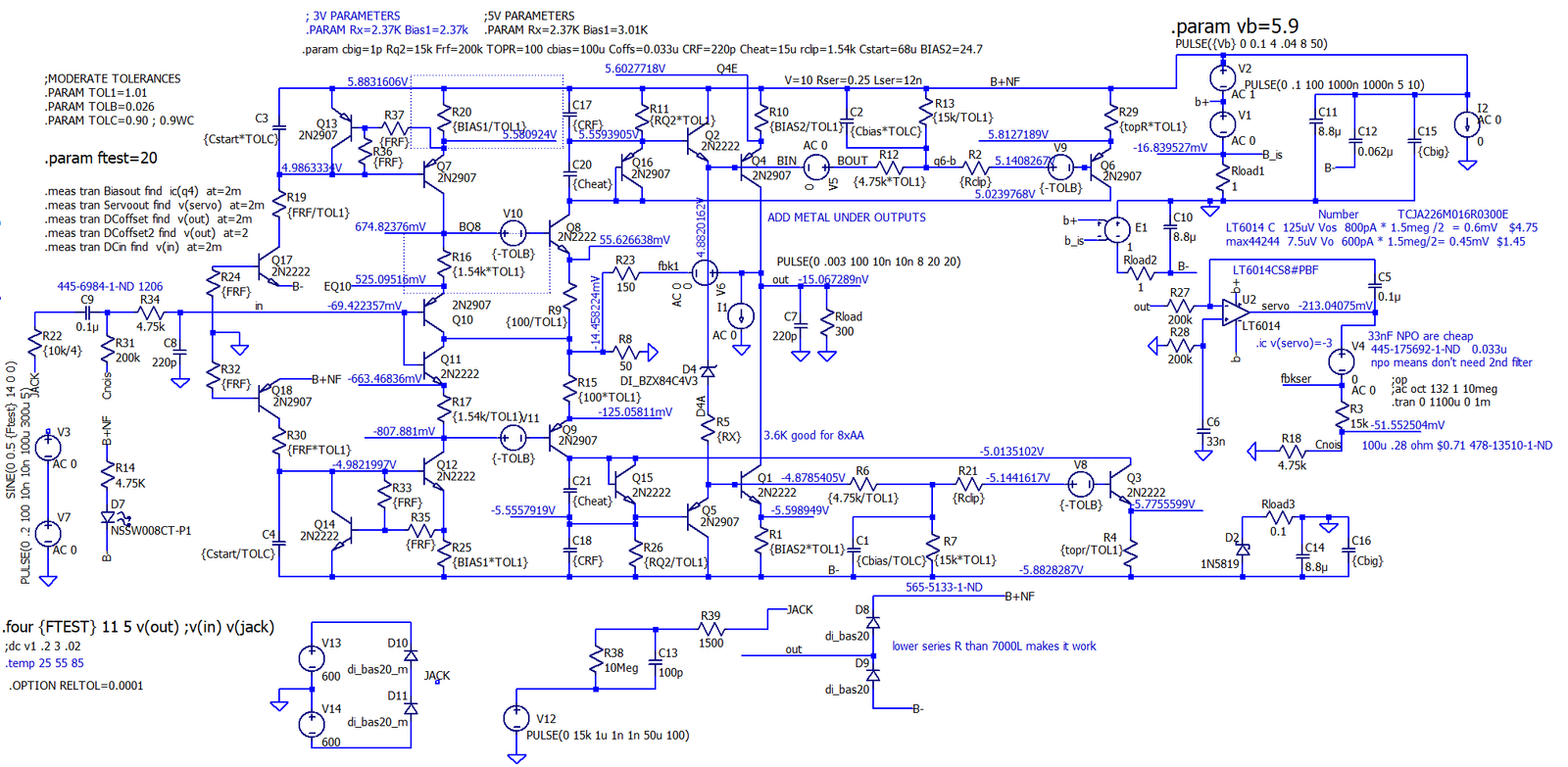
ESD applied to an unprotected input pot results in the Transistors being degraded (damaged.) This is mostly because the Vbe voltage is reversed by more than 5-6V. So if the spark gaps don't trigger at 600Vpk, the transistors are damaged.
If the input spark gaps do trigger at 600V or lower, we are protected on the input

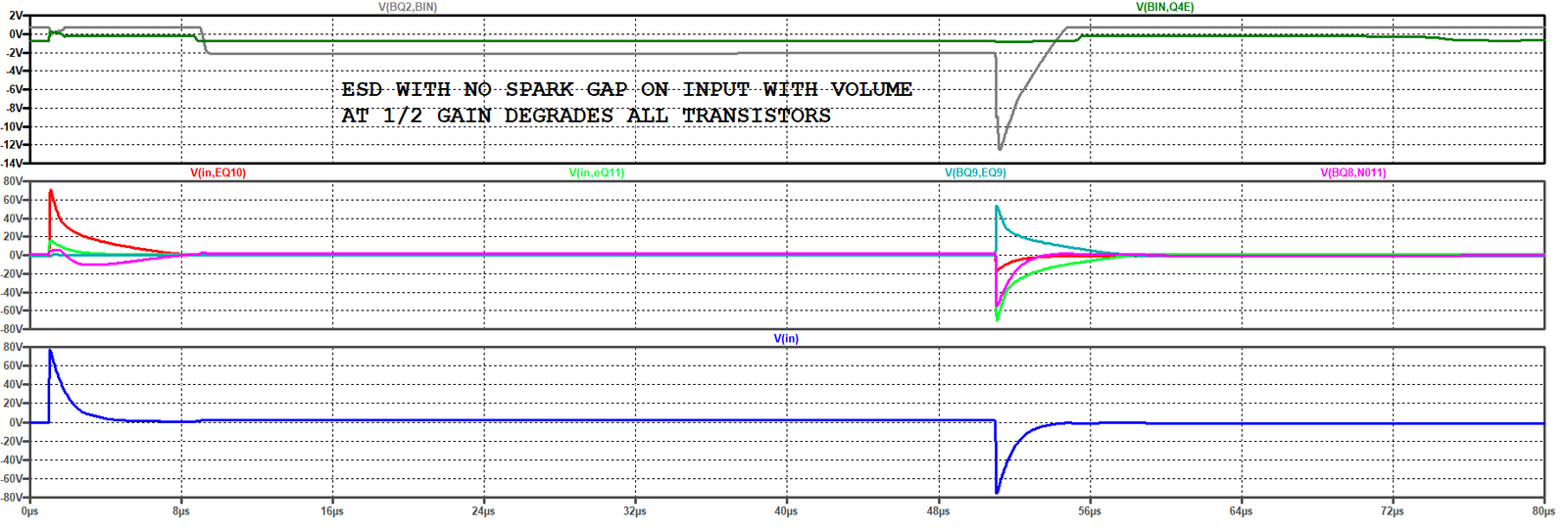
I still believe it will take some effort to ESD the output, but if it is ESD'd, the amp will be degraded.
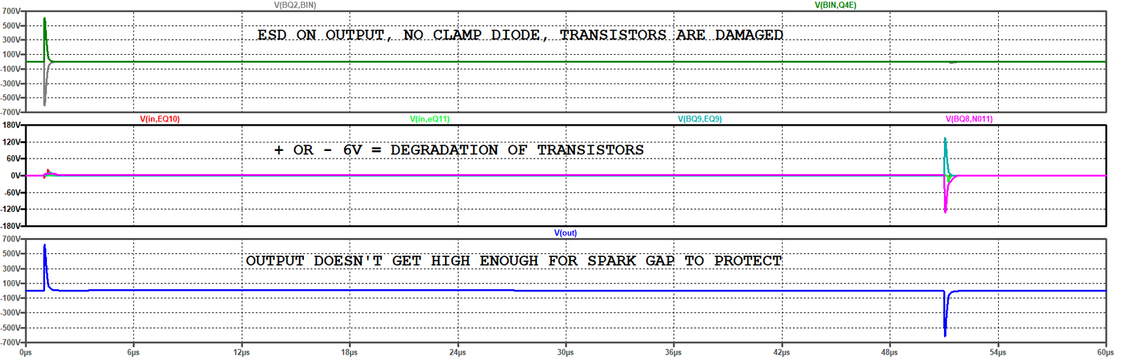
With low series R diodes on the output clamping to the power rail, the output is protected
.
Question: Will the output clamp BAT20 survive ESD? (Yes)
We are putting in 10 amps (15kV/1500 ohm) for 150nsec (1500 ohm 100pF) for an I^2*t of 15E-6 A^2T into the amp. Most of this will flow through the clamp diode. The BAS299 is rated for 9Apk for 1usec or 81E-6 A^2T. This is a 5:1 margin which is great. We could even drop down to a diode to 4A pk for 1usec on an Alternate part. The biggest thing on the alternate part is that it has to have a low internal series resistance. This resistance is the resistance that is in series with an ideal diode. An MMBD7000L won't protect against ESD.
I don't have the thermal modeling software available to give a clean calculation of the temperature rise of the output transistors. We'll have to look at a couple data sheets and make an assumption of what is allowed. There are multiple Rth Junction to Ambients given for the 2N2222A / 2N2907A SOT-23 parts in various documents. The junction is rated to 150C, but we don't want to use it there for long duration's. This design will be used indoors with an ambient less than 40C.
Fairchild MMBT2222A 357C/W on FR4 1.6"x1.6"x0.06" (no mention of copper coverage)
Onsemi MMBT2222AL 556C/W on FR5 1.0"x"0..75"x0.062" (no mention of copper coverage)
Onsemi MMBT2222AL 417C/W on Alumina 0.4x0.3x0.024 (no mention of copper coverage)
A SOT-23 was placed in the middle of a double-sided board in the center of a 28.9mm square copper pour. The SOT-23 lands did NOT touch the copper pour, but a narrow strip of copper extended from under the part to the edge of the board. This gave a Rth of 200C/W. That is a number I find hard to believe. This 200C/W may be the "CASE" rise of the part, not the junction rise of the part.
A different SOT-23 Temperature Test by Rohm
The test was with the part on a 12mm by 20mm by 0.8mm ( 0.47"x0.78"x0.032") board with no copper other than 3 traces as wide as the part's pads going to the part. This gave and Rth of 625C/W. We have a lot more copper on the 4 layer board than this. This number is far too conservative.
If we allow a peak 125C junction temperature with a 40C ambient, that becomes a 85C allowed rise. If we split the difference between the 357C/W Fairchild Number and the 556C/W Onsemi number, we get 456C/W. Solving the math, 85C rise/456C/W = 0.186W allowed. At 5.7V across the part (6V-0.3V), this is 32.7mA maximum we could put into the part. Because the parts are close to each other, this maximum allowed power will need to be reduced. If we half it, we are allowed 13.35 mA bias. This is higher than the ~12mA bias we want to use so the design is good to go.
During turn on transients, we could tolerate a 110C rise (more if the unit is cooler than 40C) for 0.24W peak or 42.3mA peak. Because this is a transient, a one-second turn on surge really won't have time to change the temperature of the PWB significantly so there is not too much risk with this number other than increased solder fatigue from temperature cycling. ( Yes, you can damage solder joint from temperature cycling. I've seen the pictures, but didn't do the math myself.)
I used an old headphone performance list I had, added a few newer headphones and ran the math on getting 110dB peak out of the headphone while allowing the peak output current to be 4x the bias current. The sound is the best at a peak current of 2x the bias current, but at 4X and 110dB, my ears are likely distorting enough not to hear the increase in 3rd harmonic that occurs when leaving the "Class A" region. Also, above 4X the bias current, the output "auto bias" circuit drifts too much and the amplifier becomes a class B amp and saying class B doesn't sound very good is being polite. I'm comfortable with this because I own a nice push pull audio (not guitar) tube amp that does the same thing with shifting of the bias when it is driven hard. If you drive it too hard, it's bias point shifts and it doesn't sound good for about a second or so after the transient. The the pushing too hard also doesn't sound good. These "not sounding good" events occur nearly at the same time. So as my friend chastised me: "GET OVER IT."
In the table below I, these are headphones that could get to within 3dB of 110dB peak with four total AA batteries (+/- 2.5V rails.) The table tells us that the amp would need at least 10.7mA bias to meet the 4X peak current to bias current criteria. With a 0.707 peak input voltage (0.5V rms) we'll want a voltage gain of 4, maybe 5.
| Peak SPL |
Vpk input | Rdrop | Vswing Available | Class A factor | Vsat driver | ||||||
| 110.0 | 0.707 | 25.0 | 4.8 | 4.0 | 0.3 |
Assuming a +/- 2.5V battery
| Manufacturer | Model | dB/ mW | Ohm | mW for dB | pk needed Volts | pk mA | Gain for V pk | Vbat needed | Db Output Avail |
Ibias mA for Ipk/Class A factor | dB margin |
| Aiwa | HP-AK100 | 100 | 16 | 10.0 | 0.57 | 35.36 | 0.80 | 1.70 | 117 | 9.5 | 6.8 |
| Aiwa | HP-J9 | 105 | 16 | 3.2 | 0.32 | 19.88 | 0.45 | 1.07 | 122 | 5.4 | 11.8 |
| Aiwa | HP-X1000 | 104 | 40 | 4.0 | 0.56 | 14.11 | 0.80 | 1.17 | 121 | 4.2 | 10.8 |
| AKG | K240 Studio | 91.4 | 55 | 72.4 | 2.82 | 51.30 | 3.99 | 4.35 | 108 | 8.3 | -2.2 |
| AKG | K271 Studio / K240S | 91 | 55 | 79.4 | 2.96 | 53.74 | 4.18 | 4.55 | 107 | 8.3 | -2.6 |
| AKG | K280 | 92 | 75 | 63.1 | 3.08 | 41.02 | 4.35 | 4.35 | 108 | 7.1 | -2.2 |
| AKG | K501 | 94 | 120 | 39.8 | 3.09 | 25.76 | 4.37 | 3.99 | 109 | 5.6 | -1.4 |
| Audio Technica | ATH-50M | 99 | 38 | 12.6 | 0.98 | 25.74 | 1.38 | 1.87 | 116 | 7.7 | 5.9 |
| Audio Technica | ATH-AD10 | 101 | 38 | 7.9 | 0.78 | 20.45 | 1.10 | 1.54 | 118 | 6.1 | 7.9 |
| Audio Technica | ATH-M30 | 100 | 65 | 10.0 | 1.14 | 17.54 | 1.61 | 1.83 | 116 | 5.8 | 6.1 |
| Audio Technica | ATH-M3x | 100 | 32 | 10.0 | 0.80 | 25.00 | 1.13 | 1.68 | 117 | 7.3 | 7.0 |
| Audio Technica | ATH-M40fs | 100 | 60 | 10.0 | 1.10 | 18.26 | 1.55 | 1.80 | 116 | 5.9 | 6.2 |
| Audio Technica | ATH-M50 | 99 | 38 | 12.6 | 0.98 | 25.74 | 1.38 | 1.87 | 116 | 7.7 | 5.9 |
| Audio Technica | ATH-M50x | 101.2 | 38 | 7.6 | 0.76 | 19.99 | 1.07 | 1.51 | 118 | 5.9 | 8.1 |
| Audio Technica | ATH-P3 | 98 | 22 | 15.8 | 0.84 | 37.96 | 1.18 | 2.03 | 115 | 10.5 | 5.0 |
| Audio Technica | ATH-W1000 | 100 | 40 | 10.0 | 0.89 | 22.36 | 1.26 | 1.70 | 117 | 6.7 | 6.8 |
| Audio Technica | ATH-W2002 | 102 | 40 | 6.3 | 0.71 | 17.76 | 1.00 | 1.40 | 119 | 5.3 | 8.8 |
| Betron | B25 | 110 | 16 | 1.0 | 0.18 | 11.18 | 0.25 | 0.71 | 127 | 3.0 | 16.8 |
| Beyerdynamic | DT-211 | 118 | 40 | 0.2 | 0.11 | 2.82 | 0.16 | 0.43 | 135 | 0.8 | 24.8 |
| Beyerdynamic | DT-770 Pro DT 990 Pro | 96 | 250 | 25.1 | 3.54 | 14.18 | 5.01 | 4.15 | 108 | 4.1 | -1.8 |
| Beyerdynamic | DT-911 | 115 | 250 | 0.3 | 0.40 | 1.59 | 0.56 | 0.69 | 127 | 0.9 | 17.2 |
| Denon | AH-D7000 | 108 | 25 | 1.6 | 0.28 | 11.26 | 0.40 | 0.81 | 125 | 3.2 | 15.0 |
| Denon | AH-D950 | 106 | 30 | 2.5 | 0.39 | 12.94 | 0.55 | 0.96 | 123 | 3.7 | 13.0 |
| Denon | AH-G500 | 103 | 28 | 5.0 | 0.53 | 18.92 | 0.75 | 1.25 | 120 | 5.4 | 10.0 |
| Etymotic | ER-4S | 98 | 100 | 15.8 | 1.78 | 17.80 | 2.52 | 2.48 | 113 | 6.1 | 3.1 |
| Fostex | T-5 | 96 | 44 | 25.1 | 1.49 | 33.79 | 2.10 | 2.58 | 113 | 9.2 | 2.7 |
| Fostex | T-7 | 98 | 70 | 15.8 | 1.49 | 21.28 | 2.11 | 2.27 | 114 | 7.2 | 3.9 |
| Grado | HP1 | 96 | 40 | 25.1 | 1.42 | 35.44 | 2.00 | 2.55 | 113 | 9.6 | 2.8 |
| Grado | SR325x | 98 | 38 | 15.8 | 1.10 | 28.88 | 1.55 | 2.07 | 115 | 8.6 | 4.9 |
| Grado | SR325e | 100 | 32 | 10.0 | 0.80 | 25.00 | 1.13 | 1.68 | 117 | 7.3 | 7.0 |
| Grado | SR80 | 94 | 32 | 39.8 | 1.60 | 49.88 | 2.26 | 3.09 | 111 | 10.7 | 1.0 |
| JVC-Victor | HP-D7 | 106 | 52 | 2.5 | 0.51 | 9.83 | 0.72 | 1.01 | 122 | 3.1 | 12.5 |
| Koss | A-250 | 98 | 60 | 15.8 | 1.38 | 22.98 | 1.95 | 2.20 | 114 | 7.5 | 4.2 |
| Koss | R-10 | 103 | 60 | 5.0 | 0.78 | 12.93 | 1.10 | 1.35 | 119 | 4.2 | 9.2 |
| Koss | TD-75 | 95 | 150 | 31.6 | 3.08 | 20.53 | 4.36 | 3.84 | 109 | 5.1 | -1.1 |
| Koss | The Plug | 112 | 16 | 0.6 | 0.14 | 8.88 | 0.20 | 0.61 | 129 | 2.4 | 18.8 |
| Pioneer | HDJ-1000 | 107 | 40 | 2.0 | 0.40 | 9.99 | 0.57 | 0.90 | 124 | 3.0 | 13.8 |
| Pioneer DJ | HDJ-X10 | 106 | 32 | 2.5 | 0.40 | 12.53 | 0.57 | 0.96 | 123 | 3.6 | 13.0 |
| Sennheiser | HD 800 | 97 | 300 | 20.9 | 3.54 | 11.80 | 5.01 | 4.09 | 108 | 3.9 | -1.6 |
| Sennheiser | HD 800 S | 96.8 | 300 | 21.0 | 3.55 | 11.84 | 5.02 | 4.10 | 108 | 3.9 | -1.7 |
| Sennheiser | HD-280 Pro | 95 | 64 | 32.4 | 2.04 | 31.80 | 2.88 | 3.08 | 111 | 7.7 | 1.0 |
| Sennheiser | HD-490II | 94 | 70 | 39.8 | 2.36 | 33.73 | 3.34 | 3.45 | 110 | 7.3 | -0.1 |
| Sennheiser | HD-600/ 580 | 97 | 300 | 20.0 | 3.46 | 11.53 | 4.89 | 4.00 | 109 | 3.9 | -1.4 |
| Sennheiser | HD-650 | 98 | 300 | 16.7 | 3.17 | 10.55 | 4.48 | 3.68 | 109 | 3.9 | -0.7 |
| Sony | MDR-7506 | 102.0 | 63 | 6.3 | 0.89 | 14.16 | 1.26 | 1.50 | 118 | 4.7 | 8.1 |
| Sony | MDR-CD1000 | 104 | 32 | 4.0 | 0.50 | 15.77 | 0.71 | 1.15 | 121 | 4.6 | 11.0 |
| Sony | MDR-CD3000 | 104 | 32 | 4.0 | 0.50 | 15.77 | 0.71 | 1.15 | 121 | 4.6 | 11.0 |
| Sony | MDR-CD780 | 106 | 32 | 2.5 | 0.40 | 12.53 | 0.57 | 0.96 | 123 | 3.6 | 13.0 |
| Sony | MDR-F1 | 100 | 12 | 10.0 | 0.49 | 40.82 | 0.69 | 1.76 | 116 | 10.8 | 6.5 |
| Sony | MDR-V900DJ | 107 | 24 | 2.0 | 0.31 | 12.89 | 0.44 | 0.88 | 124 | 3.6 | 14.0 |
| SoundMagic | E80 | 102 | 64 | 6.3 | 0.90 | 14.04 | 1.27 | 1.50 | 118 | 4.6 | 8.1 |
| Stanton | DJ PRO 50 S | 98 | 32 | 15.8 | 1.01 | 31.47 | 1.42 | 2.04 | 115 | 9.1 | 5.0 |
| Stanton | SRS-215 | 98 | 50 | 15.8 | 1.26 | 25.18 | 1.78 | 2.14 | 115 | 7.9 | 4.5 |
| Stanton | SRS-275 | 101 | 100 | 7.9 | 1.26 | 12.60 | 1.78 | 1.83 | 116 | 4.7 | 6.1 |
| Technics | RP-DJ700 | 105 | 56 | 3.2 | 0.60 | 10.63 | 0.84 | 1.11 | 121 | 3.4 | 11.4 |
| Ultimate Ears | TripleFi 10 | 117 | 32 | 0.2 | 0.11 | 3.53 | 0.16 | 0.45 | 134 | 1.0 | 24.0 |
| Ultrasone | Edition 10 | 99 | 32 | 12.6 | 0.90 | 28.05 | 1.27 | 1.85 | 116 | 8.1 | 6.0 |
| Yamaha | CH10 | 91 | 32 | 79.4 | 2.25 | 70.46 | 3.19 | 4.27 | 108 | 10.7 | -2.0 |
| Yamaha | RH3 | 95 | 60 | 31.6 | 1.95 | 32.47 | 2.75 | 3.01 | 111 | 7.9 | 1.2 |
| Yamaha | RH5MA | 98 | 32 | 15.8 | 1.01 | 31.47 | 1.42 | 2.04 | 115 | 9.1 | 5.0 |
-
If we use 8 AA batteries instead of 4, with the same bias current, we pick up being able to drive these headphones if we can get a bit more than 0.5Vrms input voltage.
| Peak SPL |
Vpk input | Rdrop | Vswing Available | Class A factor | Vsat driver | ||||||
| 110.0 | 0.707 | 25.0 | 4.8 | 4.0 | 0.3 |
| Manufacturer | Model | dB/ mW | Ohm | mW for dBpk | pk Volts | pk mA | Gain for V pk | Vbat needed | Db Output Avail | Pk/ Class A Ibias mA | dB margin |
| AKG | K141M | 98 | 600 | 15.8 | 4.36 | 7.27 | 6.17 | 4.79 | 113 | 6.8 | 3.4 |
| Beyerdynamic | DT-990 | 96 | 600 | 25.1 | 5.49 | 9.15 | 7.76 | 5.97 | 111 | 6.8 | 1.4 |
| Koss | PRO/4AA | 94 | 230 | 39.8 | 4.28 | 18.61 | 6.05 | 4.99 | 113 | 9.0 | 3.0 |
| Sennheiser | HD-540II | 94 | 300 | 39.8 | 4.89 | 16.29 | 6.91 | 5.54 | 112 | 8.2 | 2.1 |
If we use 8 AA batteries instead of 4 and double the bias current, we pick up these headphones. The output transistors will be running at 99C with a 40C ambient (40C inside the box, not at your chair.) That is very hot, but the design will survive. I would prefer to not increase the bias current all the way to 23mA, but may be increase it by 50% to about 17mA by changing the four 24.9 ohm resistors to 16.9 ohm.)
| Manufacturer | Model | dB/ mW | Ohm | mW for dBpk | pk Volts | pk mA | Gain for V pk | Vbat needed | Db Output Avail | Pk/ Class A Ibias mA | dB margin |
| Audeze | LCD-2 | 91 | 60 | 79.4 | 3.09 | 51.46 | 4.37 | 4.62 | 114 | 16.7 | 3.7 |
| Beyerdynamic | DT-431 | 86 | 40 | 251.2 | 4.48 | 112.07 | 6.34 | 7.53 | 109 | 20.4 | -0.7 |
| HiFiMAN | HE-5LE | 87.5 | 38 | 177.8 | 3.68 | 96.74 | 5.20 | 6.34 | 111 | 20.9 | 0.8 |
| HiFiMAN | HE-6 | 83.5 | 50 | 446.7 | 6.68 | 133.67 | 9.45 | 10.28 | 107 | 18.3 | -3.5 |
| Koss | R-200 | 84 | 60 | 398.1 | 6.91 | 115.20 | 9.77 | 10.04 | 107 | 16.7 | -3.3 |
| Yamaha | RH1 | 90 | 32 | 100.0 | 2.53 | 79.06 | 3.58 | 4.76 | 113 | 22.6 | 3.5 |
| AKG | K240 Studio | 91.4 | 55 | 72.4 | 2.82 | 51.30 | 3.99 | 4.35 | 114 | 16.4 | 4.3 |
| AKG | K271 Studio / K240S | 91 | 55 | 79.4 | 2.96 | 53.74 | 4.18 | 4.55 | 114 | 17.1 | 3.9 |
| AKG | K280 | 92 | 75 | 63.1 | 3.08 | 41.02 | 4.35 | 4.35 | 114 | 14.1 | 4.3 |
| Grado | SR80 | 94 | 32 | 39.8 | 1.60 | 49.88 | 2.26 | 3.09 | 117 | 14.5 | 7.5 |
| Yamaha | CH10 | 91 | 32 | 79.4 | 2.25 | 70.46 | 3.19 | 4.27 | 114 | 20.4 | 4.5 |
These two headphone need a power amp to generate enough
voltage to drive them. Don't bother trying to adjust this amp to drive
these to 110dBpk.
| Manufacturer | Model | dB/ mW | Ohm | mW for dBpk | pk Volts | pk mA | Gain for V pk | Vbat needed | Db Output Avail | Pk/ Class A Ibias mA | dB margin |
| AKG | AKG K1000 | 74 | 120 | 3981.1 | 30.91 | 257.59 | 43.71 | 37.60 | 95 | 11.9 | -14.9 |
| AKG | K240M | 88 | 600 | 158.5 | 13.79 | 22.98 | 19.50 | 14.62 | 103 | 6.8 | -6.6 |
We don't want the gain set resistor to be changing with output voltage (power loss) To limit this, the 150 ohm "gain set" resistor should be a 25ppm/C part. The 50 ohm to ground sees 1/4 the voltage or 1/16 the power. It will be OK at 100ppm/C. But if you want, go a head and make it 25ppm/C too.
This is a different type of issue than Class II ceramics (X7R etc.) being micro-phonic and not sounding good if used in the signal path. NPO ceramic capacitors are not microphonic and typically sound good.
The first issue is failures from micro-cracks in the ceramic body of the capacitor.
I normally start to see SMT capacitors crack from mechanical strain occur at the 1210 size. The 1210's do require a bit of effort to break, such as snapping a PBA out of its carrier instead of cutting the carrier off with the cap near the break out point or being used insind a high vibration vehicle. I have a friend who has had issues with SMT caps larger than 1812 because of cracking/crazing just from temperature cycling. (i.e. 1825 doesn't work; but 1812 passes.)
A general rule is to keep 1210 and larger caps three PB thicknesses away from any mechanical connections and the edge of any heavy part. We also place the part so the 1210 would bends across the short edge, not the long edge.
A second related issue is violent ceramic capacitor failures.
I've personally had stacked ceramics "explode" (Oops, I forgot to call it "Rapidly Disassemble with a Passion") in high current circuits because the surface cracked and the crack generated a short. If I didn't have PPE on, I would have been hurt (not could have, would have.) Ceramic caps with high CV products have thin dielectric layers that break easily in soldering and handling. Some of the new high CV product capacitors have very thin ceramic layers. They even crack from the thermal shock of soldering. Avoid the SMT ceramics with low voltage ratings because of this increase in cracking risk. Usually, if the part is rated for automotive use, it is lower risk than the same foot print part and value that is rated for general use. A coated ceramic X7R is lower risk than a part of the same size and voltage ratings because the surfaces are protected; the risk is still there, it is just many times lower.
A third issue is value drift on Class 2 ceramics ( X7R drifts, NPO does not.)
The temperature variation in X7Rs capacitor value is large. There also is a drop in capacitor value with DC bias. Then there is a 4-8% drop in value per decade hour of existence. i.e. 8% * log10 (hours of existence, powered or not.) The high CV product parts tend to run closer to the 8% change, the older CK05/CK06 military ceramics and commercial parts of same size tend to run closer to the 4% change. -8% * log10(10 years * 8000hr/yr) = -39.2% (-44% change in value occurs in 39 years) These three issues are additive. A 10% change from temperature plus 20% drop from DC bias plus 40% drop from aging says we only have 30% of the original value left.
This part drift with age is real. My cube mate at work got bit by it.
A fourth issue is self heating. NPO and N1500 capacitors usually don't have this issue. Self heating is the big issue with AC on X7R capacitors. The issue is that the capacitor gets hot.
Looking at two parts from digikey, we have two HV ceramics in 1812 (we won't even consider the 1825 size parts). One is a 0.1u 1kV 1812Y1K00104KST (Knowles/ Johanson MFG) and the other is a 39nF 1812J1K50393KXT in 1500kV. Both over $3 each.
The pads for these run 96 mils apart which would make them closer to 860Vpk, 608Vrms best case allowed voltage on the parts.
From "AC Power Computations for DC Rated Capacitors" by Johanson Dielectrics the 1812 capacitor can handle 0.4W at 25C. At 85C this drops to (125-85C)/(125-25C) = 0.16W allowed. The dissipation curves below are from the same Johanson Dielectrics source.
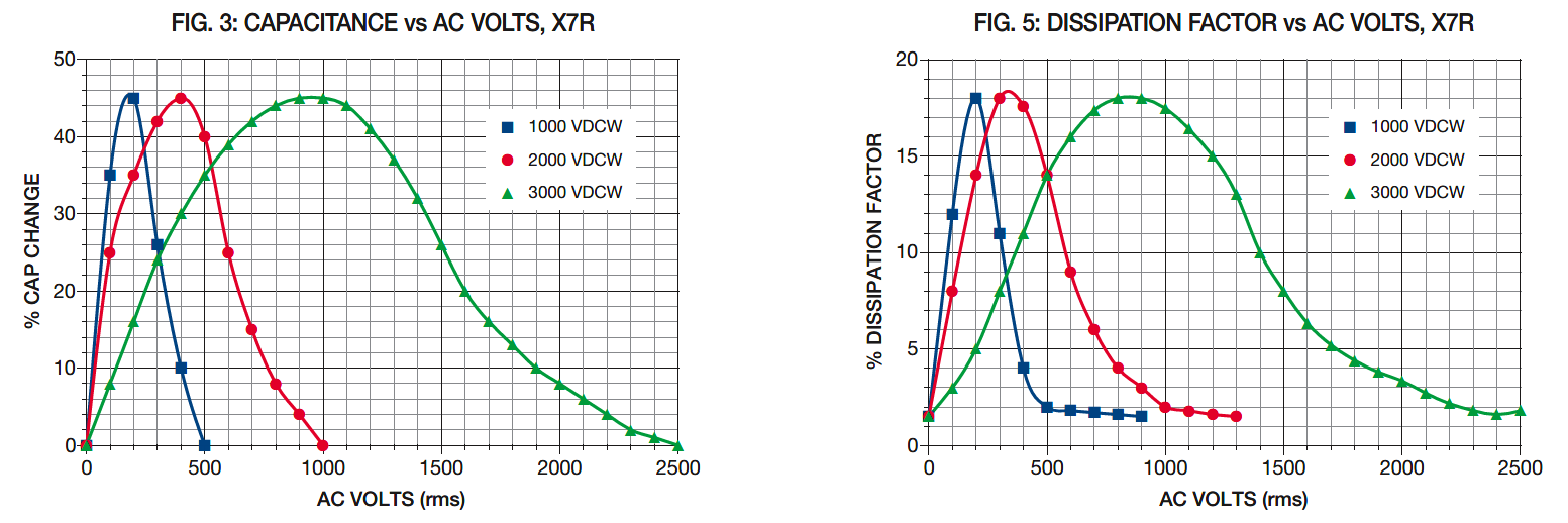
With the 39nF 1500V, we can get 210Vrms at 60Hz. Two capacitors in series per row and two rows in parallel give 39nF at 420Vrms at high line, unloaded. This amount of allowed voltage is to low for $12 of parts that we may need to add even more parts to cover part shifts due to aging etc.
With the 100nF 1000V, we can get 122Vrms at 60Hz. Three caps in series give 33nF (enough to run without an LED) and 366Vrms at high line, unloaded. Again the allowed voltage is low for $11.70 in parts that could easily "self destruct" from soldering and mechanical stresses causing micro-cracks.
| 1000V used at RMS |
%change value | %dissipation | Cap | Tol Cap | Freq | PWR | Scale Voltage by 0.16W |
| 100 | 35.00% | 12.00% | 1.00E-07 | 10.00% | 60 | 0.067 | 154 |
| 200 | 45.00% | 18.00% | 1.00E-07 | 10.00% | 60 | 0.433 | 122 |
| 400 | 10.00% | 4.00% | 1.00E-07 | 10.00% | 60 | 0.292 | 296 |
| 2000V used at |
%change value | %dissipation | Cap | 10.00% | Freq | PWR | |
| 100 | 25.00% | 8.00% | 1.00E-07 | 10.00% | 60 | 0.041 | 196 |
| 200 | 35.00% | 14.00% | 1.00E-07 | 10.00% | 60 | 0.314 | 143 |
| 400 | 45.00% | 18.50% | 1.00E-07 | 10.00% | 60 | 1.780 | 120 |
| 100 | 25.00% | 8.00% | 3.90E-08 | 10.00% | 60 | 0.016 | 315 |
| 200 | 35.00% | 14.00% | 3.90E-08 | 10.00% | 60 | 0.122 | 229 |
| 400 | 45.00% | 18.50% | 3.90E-08 | 10.00% | 60 | 0.694 | 192 |
| Average 1k 2k For 1.5kV |
%change value | %dissipation | Cap | 10.00% | Freq | PWR | |
| 100 | 30.00% | 10.00% | 3.90E-08 | 10.00% | 60 | 0.021 | 276 |
| 200 | 40.00% | 16.00% | 3.90E-08 | 10.00% | 60 | 0.145 | 210 |
| 400 | 27.50% | 11.25% | 3.90E-08 | 10.00% | 60 | 0.371 | 263 |
The DC offset control parts on this card should be clean of flux, oils and fingerprints. If conformal coating the board, it needs to be first dried and then conformal coated. The drying can occur from a 60-80C bake out in a PLA filament dryer or wrap the PBA in foil and baked it at 70C (158F) sandwiched between two cooking pans in a toaster oven.
Reused table from a different design:
In the design, I'll follow the trace spacing from the "Old Engineer Rule" for conformal coated spacing. This Old Engineer guide has been working for decades. I trust it more than IPC. I've had failures between traces closer than 10 mils (a distance that was allowed by IPC) in the past at voltages as low as 15V, so the B1 spacing for use from IPC on power products are suspect in my book. For uncoated, I'll use the greater of IPC B2 and twice the Old Engineer's rule.
At beginning of life on a perfectly clean board, the board will support higher voltages than given by IPC. At 1100 feet altitude, a 50 mil gap arcs at 1500Vac (2121Vpk) 60Hz and a 60 mil gap does not. Don't expect that level of performance after a few years of dust, finger prints and humidity.
| . | Internal | External UnCoated |
External Coated |
. | External Uncoated |
Internal + coated | Web Article | |
| IPC B1 | IPC B2 | IPC B4 | 5V/Mil | Old Eng Rule | 100V/mil | |||
| Vpk | mils | Mils | Mils | Skip 10mil | 10V/mil + 10mil |
Layer to Layer | ||
| 2000 | 157.5 | 394 | 212 | 400 | 210 | 20 | ||
| 1800 | 137.8 | 354 | 188 | 360 | 190 | 18 | ||
| 1200 | 78.7 | 236 | 116 | 240 | 130 | 12 | ||
| 1000 | 59 | 197 | 92 | 200 | 110 | 10 | ||
| 800 | 39.4 | 158 | 68 | 160 | 90 | 8 | ||
| 600 | 19.7 | 118 | 44 | 120 | 70 | 6 | ||
| 301 | 9.84 | 99 | 32 | 60.2 | 40.1 | 3.01 | ||
| 15 | 1.97 | 4 | 2 | 3 | 11.5 |
Here is the same table with dimension in mm instead of 1/1000 (mil) of an inch
| . | Internal | External UnCoated |
External Coated |
External Uncoated |
Internal + coated | Web Article | ||
| IPC B1 | IPC B2 | IPC B4 | 5V/Mil | Old Eng Rule | 100V/mil | |||
| Vpk | mm | mm | mm | in mm | mm | mm | ||
| 2000 | 4.00 | 10.01 | 5.38 | 10.16 | 5.33 | 0.51 | ||
| 1200 | 2.00 | 5.99 | 2.95 | 6.10 | 3.30 | 0.30 | ||
| 1000 | 1.50 | 5.00 | 2.34 | 5.08 | 2.79 | 0.25 | ||
| 800 | 1.00 | 4.01 | 1.73 | 4.06 | 2.29 | 0.20 | ||
| 600 | 0.50 | 3.00 | 1.12 | 3.05 | 1.78 | 0.15 | ||
| 300 | 0.25 | 2.51 | 0.81 | 1.53 | 1.02 | 0.08 | ||
| 15 | 0.05 | 0.10 | 0.05 | 0.08 | 0.29 |
Trace Widths for 1A RMS:
| 0.5 Oz CU With 1 Oz plate 5C rise |
1 OZ 5C Rise |
0.5 Oz CU 1 Oz plate 5C rise |
1 OZ 5C Rise |
||
| A rms | External mil | Internal mil | External mm | Internal mm | |
| 1 | 16 | 24 | 0.41 | 0.61 | |
| 1 Sec Fusing | 5.45 Arms | 5.9 Arms | |||
| 2 inch Ohms | 0.0517 | 0.0477 |
Remember:
Any traces with more than 200Vpk between them should consider rounded corners on both the low voltage and high voltage sides. 270Vpk at 60Hz is the Paschen minimum for air. The Paschen minimum is the lowest voltage where air breakdown can start. It doesn't mean that breakdown occurs, it means that it can occur. At higher frequencies, the Paschen minimum voltage drops. Solder mask doesn't remove the risk, but it does help keep the effective board surfaces cleaner.
Any traces with more than 450Vpk between them, need rounded corners. I've measured air going into corona at 325Vrms (459Vpk) at room pressure.
There should be no square pads facing each other between high and low voltage. One fix is to used rounded guard traces. Guard traces on the outer layers work better than guard planes on inner layers, but If you can't fit the trace on the outer layer, make sure you but a rounded edge guard plain/trace on an inner layer. Another fix is to put rounded edges on the square pads.
We have to avoid sharp points when using high voltage. This sharp point rule is in 3D, not just in the X and Y dimensions. Corona and voltage break down issues are real. I've had to fix them in production. If you are in between a rock and a hard place on making things fit, trading a little more (not a lot) of corona risk during turn-on vs lower corona risk in normal operation is the correct choice. That does NOT mean you can use 32 mil trace spacing at 800V (unloaded) peak (should be 90mil) to pass turn-on stresses.
I prefer to use long screws to make standoffs (feet) to both support hold boards in place. The screws are easily adjustable in length and often cost less than Hex Posts.
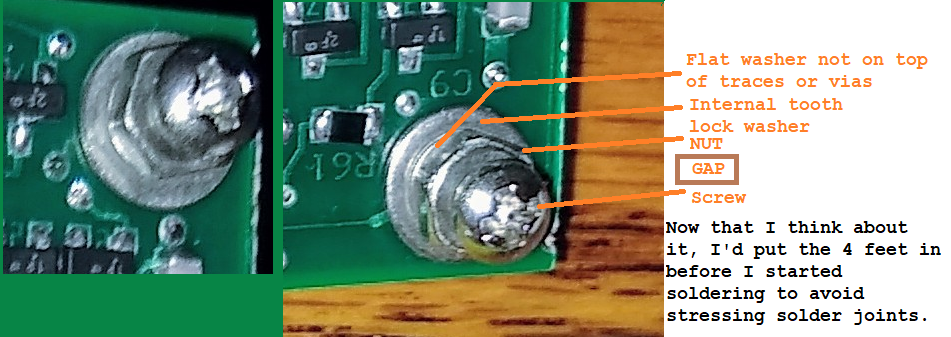
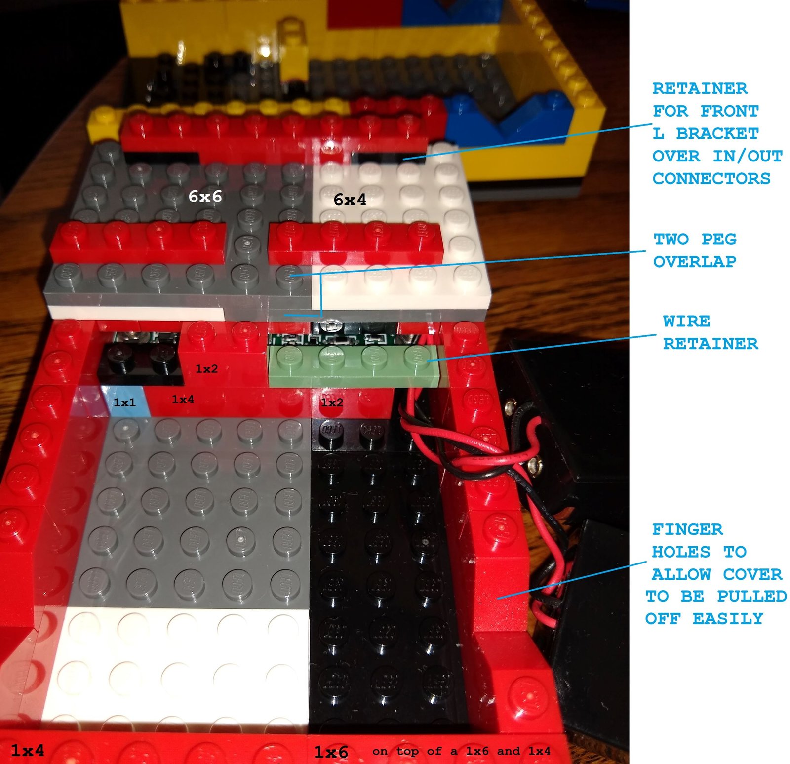
Inside the case it looks like this.
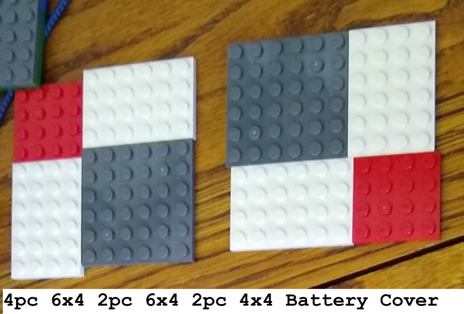
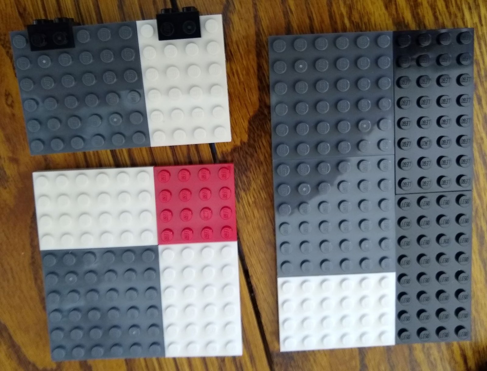
The bottom of the case is made from several flat plates stacked to make a 2 layer thick plate.

The battery cover is made is a similar fashion.
Top and bottom assembled
Under the electronic's top cover
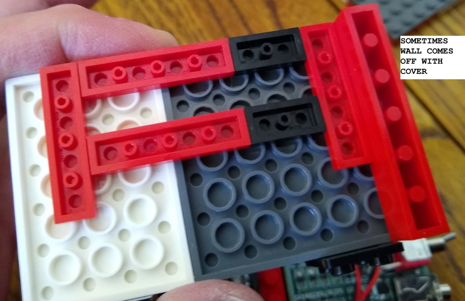
The front of the case has small Lego pieces to hold the "FEET" on the PBA in place.
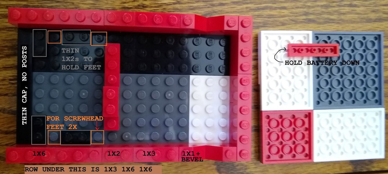
Details on building battery to electronics section.
Make sure you leave a few pieces on the floor in front of the kid's bedrooms, paybacks are heck! (Kidding. No, don't do that.)
In the appendices below I'm opening my notebook further for people who want nit pick the design. . .
If we want more voltage gain, we have to change the shunt feedback divider. The approximate voltage gain is (R25 + R28)/R28.
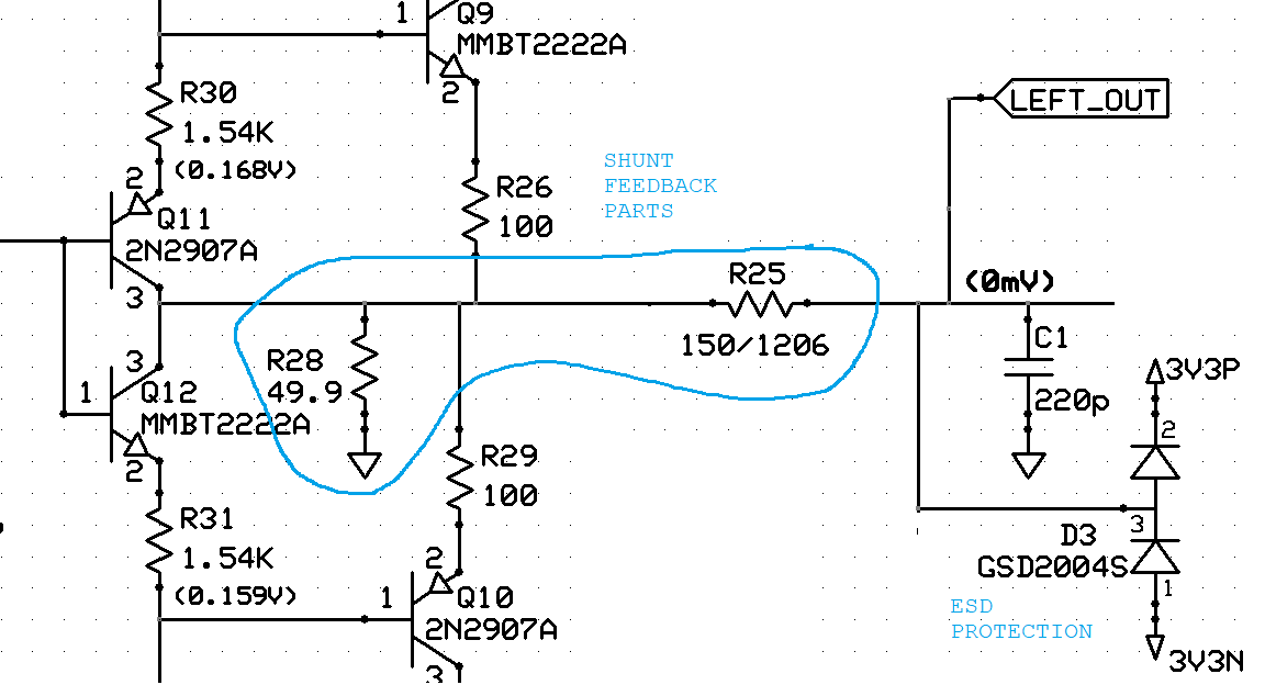
But this design depends of feedback to operate and the "There Ain't No Such Thing as a Free Variable" (TANSTAAFV) rule kicks in. For higher gain (say 7 instead of 4), which resistor should we change for minimum performance reduction? I tried 4 combinations,
50 ohm 150 ohm (the standard design.).
50 ohm 300 ohm (a gain of 7 design)
25 ohm 150 ohm (a gain of 7 design) <- The best higher gain option.
This gives Minor change (50%) in
output voltage overshoot when power is toggled ON to OFF back to ON.
Both gain of 7s had same overshoots.
17Hz gain bump slightly bigger. Output impedance is lower (better)
than with 50 ohm 300 ohm setting, but still higher than 50 ohm 150
ohm. Power Supply Noise rejection same as with 50 ohm 300 ohm setting.
Gain of 7 slightly worse than gain of 4 for PSRR
50 ohm 300 ohm (a gain of 12 design.)
Bigger change (2X) in output voltage overshoot when power is toggled
Even bigger 17Hz gain bump than gain of 7, but no real issue..
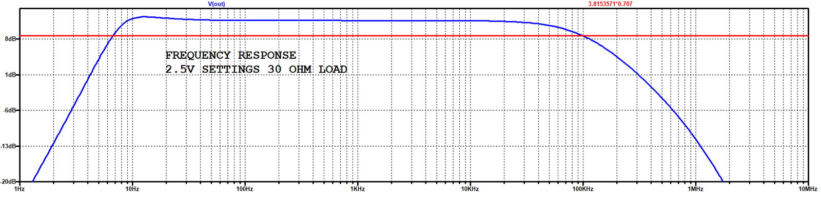
Below is a big picture comparing the results for turn on overshoots, frequency response, output impedance and PSRR.

We really shouldn't make R25, the 150 ohm, any smaller. It already dissipates 100mW peak when running from +/- 6V rails and we don't want this part to heat up because if it's value changes from heat, the output voltage will also change.
If you don’t like the gain peak at
17Hz from decreasing the 49.9 ohm resistor (R28), reduce the 4.75K to
ground in the output of the DC servo opamp by the same ratio you
reduced R28. (50 ohm to 25 ohm, 4.75K to 2.37K.) and have a voltage
gain of 7.
When the design is in CLASS A, the gain in the feedback loop does not change. When the design transistions from Class A to Class B, you typically lose 1/2 the loop gain. In Class A, for a given "Error Voltage" the top transistor can pull up by 10mA with the bottom transistor pull down LESS by 10mA. So you get a 20mA change in current to the output. In Class B, for the same "Error Voltage" the top transistor still pulls up by 10mA, but the bottom transistor does nothing. So you get a 10mA change in current when you transition into Class B.
Engineers use the term often use the term "Error Voltage" generically. The error occurs at the feedback point and the Error Voltage (or current) is the difference between where you would be with infinite loop gain (the ideal world) and where you are at (the real world.) I believe the "Error Voltage" needs to be dominated by "linear components" (resistors) not by effective resistances (the gain generated by the gate to source/cathode of a FET/Tube or Vbe of a transistor.)
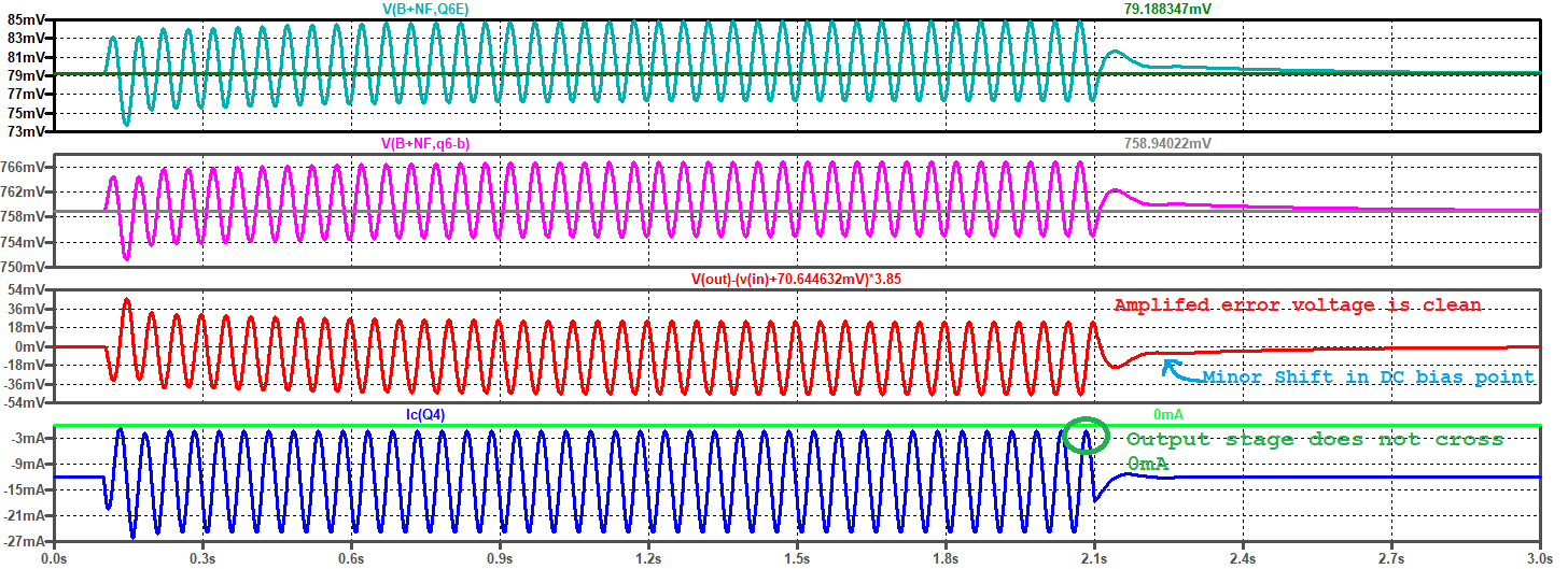
At the edge of going into class B, we get this Fourier:
RELTOL=0.00001 Time step = 100usec for 20 Hz
N-Period=5
Fourier components of V(out)
DC component:-2.30472e-008
Harmonic Frequency Fourier
Normalized
Number [Hz]
Component Component
1
2.000e+01 6.434e-01
1.000e+00
2
4.000e+01 2.975e-04 4.623e-04
3
6.000e+01 4.202e-04 6.531e-04
4
8.000e+01 9.522e-05 1.480e-04
5
1.000e+02 9.047e-05 1.406e-04
6
1.200e+02 2.911e-05 4.524e-05
7
1.400e+02 2.157e-05 3.352e-05
8
1.600e+02 7.727e-06 1.201e-05
9
1.800e+02 4.621e-06 7.182e-06
10
2.000e+02 1.519e-06 2.361e-06
11
2.200e+02 6.474e-07 1.006e-06
Total Harmonic Distortion: 0.082790%(0.082781%)
N-Period=5
Fourier components of V(in)
DC component:-0.0678156
Harmonic Frequency Fourier
Normalized
Number [Hz]
Component Component
1
2.000e+01 1.668e-01 1.000e+00
2
4.000e+01 2.839e-06 1.702e-05
3
6.000e+01 1.942e-06 1.164e-05
4
8.000e+01 2.690e-07 1.613e-06
5
1.000e+02 1.794e-07 1.075e-06
6
1.200e+02 4.355e-08 2.611e-07
7
1.400e+02 2.706e-08 1.622e-07
8
1.600e+02 9.488e-09 5.688e-08
9
1.800e+02 5.200e-09 3.118e-08
10
2.000e+02 1.357e-09
8.137e-09
11
2.200e+02 8.221e-10 4.929e-09
Total Harmonic Distortion: 0.002071%(0.001592%)
Kicking this to 200Hz and a 10usec time step we get a big improvement in the 2nd harmonic (which we really only need it below 1%) and a moderate improvement in the 3rd harmonic.
N-Period=5
Fourier components of V(out)
DC component:-2.06203e-008
Harmonic Frequency Fourier
Normalized
Number [Hz]
Component Component
1
2.000e+02 6.106e-01
1.000e+00
2
4.000e+02 3.328e-05
5.450e-05
At 20 Hz, this was
4.623e-04(normalized)18.5 dB lower
3
6.000e+02 2.436e-04 3.990e-04
At 20 Hz, this was
6.531e-04(normalized)4.3dB lower
4
8.000e+02 1.348e-05 2.208e-05
5
1.000e+03 4.523e-05
7.407e-05
At 20 Hz, this was
1.406e-04(normalized)5.5 dB lower
6
1.200e+03 3.930e-06
6.436e-06
7
1.400e+03 9.054e-06 1.483e-05
8
1.600e+03 1.020e-06
1.671e-06
9
1.800e+03 1.778e-06
2.912e-06
10
2.000e+03 2.325e-07
3.808e-07
11
2.200e+03 3.253e-07
5.327e-07
Total Harmonic Distortion: 0.041037%(0.041002%)
N-Period=5
Fourier components of V(in)
DC component:-0.0702048
Harmonic Frequency Fourier
Normalized
Number [Hz]
Component Component
1
2.000e+02 1.578e-01 1.000e+00
2
4.000e+02 1.965e-08 1.245e-07
3
6.000e+02 1.128e-07 7.145e-07
4
8.000e+02 6.028e-09
3.820e-08
5
1.000e+03 1.965e-08 1.245e-07
6
1.200e+03 1.952e-09
1.237e-08
7
1.400e+03 4.070e-09
2.579e-08
8
1.600e+03 9.867e-10
6.252e-09
9
1.800e+03 6.688e-10 4.238e-09
10
2.000e+03 5.601e-10
3.549e-09
11
2.200e+03 8.764e-10
5.554e-09
Total Harmonic Distortion: 0.000074%(0.000000%)
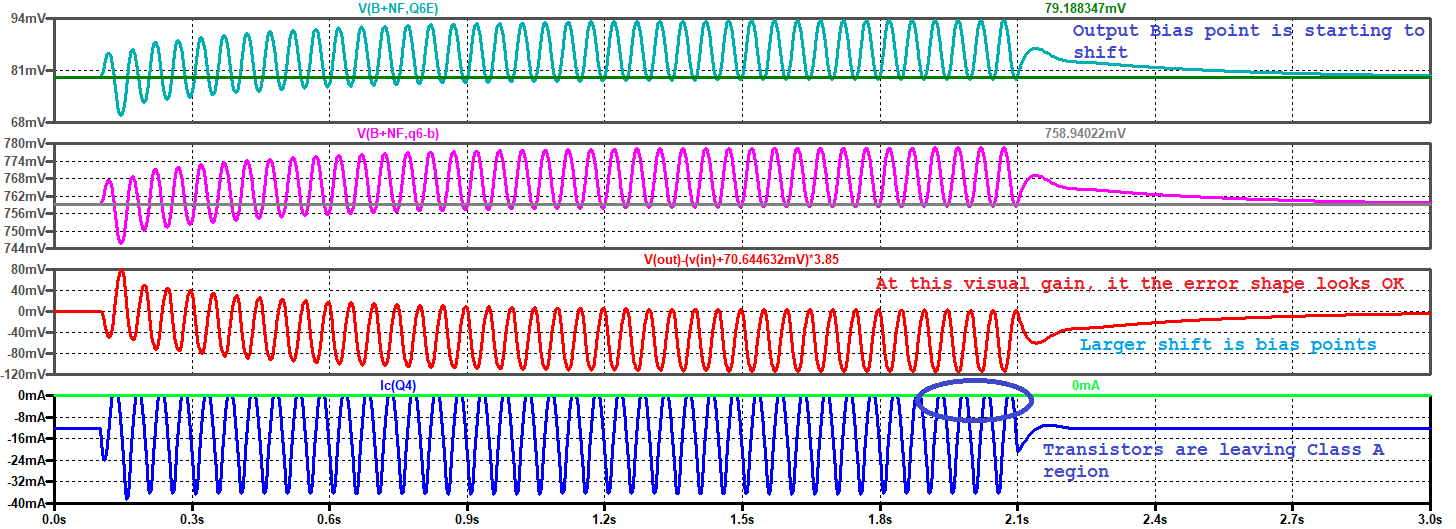
Lets increase the drive by 50% and see what happens.
N-Period=5
Fourier components of V(out) at
150% of Class A border.
DC component:-3.70282e-008
Harmonic
Frequency Fourier
Normalized
Number [Hz]
Component
Component
1
2.000e+01 9.577e-01
1.000e+00
2
4.000e+01 1.938e-03
2.024e-03
At class A border, this was 4.623e-04 (normalized)
3
6.000e+01 3.428e-03
3.580e-03
At class A border, this was 6.531e-04 (normalized
4
8.000e+01 3.855e-04
4.025e-04
5
1.000e+02 2.395e-04
2.501e-04
6
1.200e+02 2.304e-04
2.406e-04
7
1.400e+02 2.731e-04
2.852e-04
8
1.600e+02 8.691e-05
9.076e-05
9
1.800e+02 4.300e-05
4.490e-05
10
2.000e+02 8.058e-05
8.414e-05
11
2.200e+02 5.706e-05
5.959e-05
Total Harmonic Distortion: 0.415888%(0.415932%)
N-Period=5
Fourier components of V(in) (Not a large differenc
DC component:-0.0568909
Harmonic Frequency Fourier
Normalized
Number [Hz]
Component
Component
1
2.000e+01 2.499e-01
1.000e+00
2
4.000e+01 1.843e-05
7.378e-05
3
6.000e+01 1.574e-05
6.300e-05
4
8.000e+01 1.040e-06
4.164e-06
5
1.000e+02 4.600e-07
1.841e-06
6
1.200e+02 3.665e-07
1.467e-06
7
1.400e+02 3.490e-07
1.397e-06
8
1.600e+02 9.427e-08
3.773e-07
9
1.800e+02 3.530e-08
1.413e-07
10
2.000e+02 7.178e-08
2.873e-07
11
2.200e+02 4.761e-08
1.905e-07
Total Harmonic Distortion: 0.009715%(0.009601%)
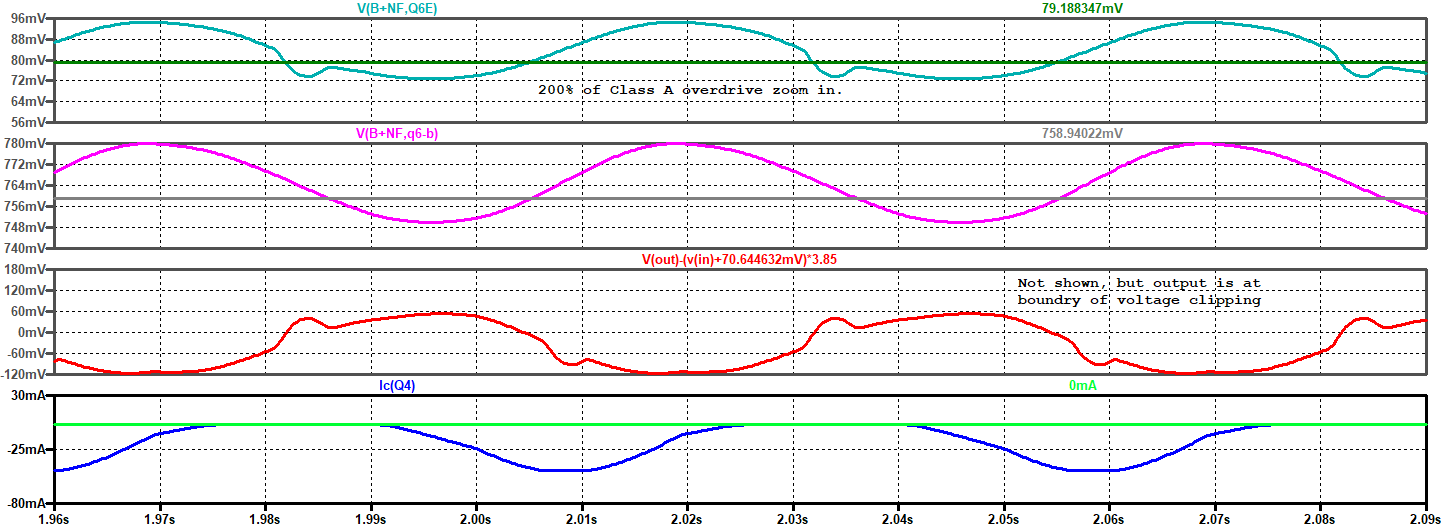
Lets go to 200% of the Class A point. We see some ugliness in the error voltage, but the bias points are still behaving.
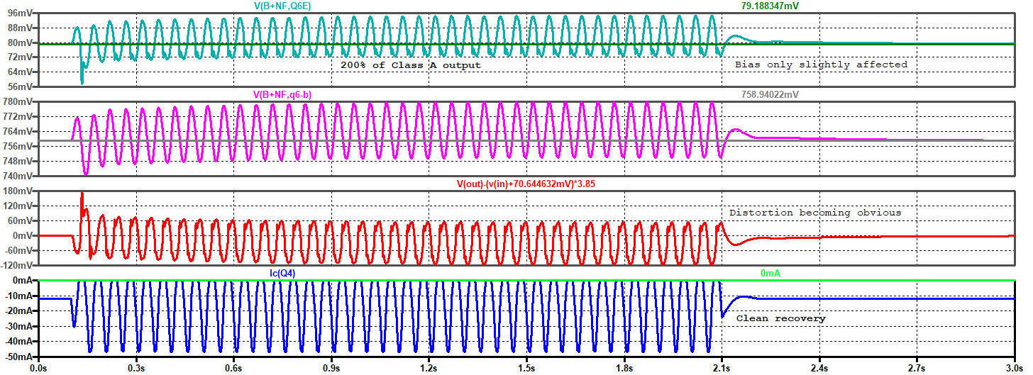
Zoom in we see at 200% "Error Voltage" is starting to be not very linear. While not shown above, the "bumps" in the "error voltage" (red trace) were not seen in the 150% run.
N-Period=5
Fourier components of V(out)
DC component:-2.8131e-008
Harmonic Frequency Fourier
Normalized
Number [Hz]
Component
Component
1
2.000e+01 1.250e+00
1.000e+00
2
4.000e+01 4.146e-03
3.318e-03
At class A border, this was 4.623e-04 (normalized) 17dB worse
3
6.000e+01 1.463e-02
1.171e-02
At class A border, this was 6.531e-04 (normalized) 17.9dB worse
4
8.000e+01 3.143e-03
2.515e-03
5
1.000e+02 7.212e-03
5.771e-03
6
1.200e+02 1.547e-03
1.238e-03
7
1.400e+02 6.695e-03
5.357e-03
8
1.600e+02 1.094e-03
8.751e-04
9
1.800e+02 4.850e-03
3.881e-03
10
2.000e+02 5.674e-04
4.540e-04
11
2.200e+02 3.152e-03
2.522e-03
Total Harmonic Distortion: 1.550247%(1.561126%)
At 300% of class A point we were voltage clipping with +/- 2.5V rails, so I increased the voltage to +/- 5V for that run. sizable
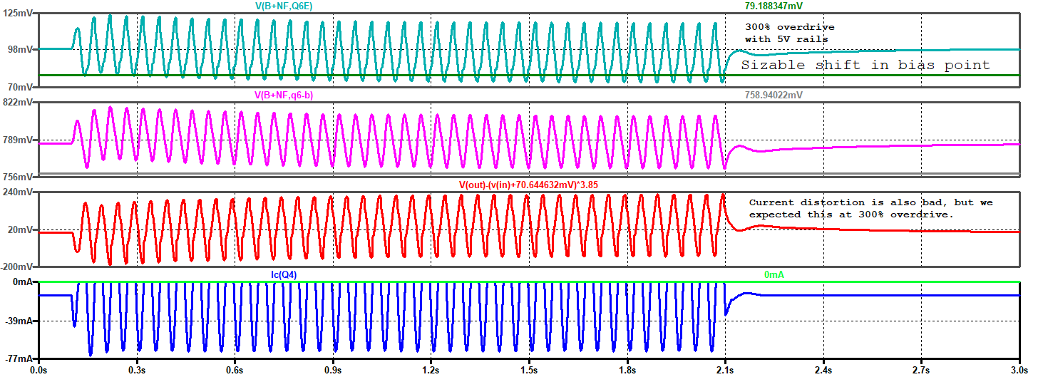
It's fun to beat up and abuse the circuit in SPICE. You don't get to smell the smoke (sigh . . .), but you don't have to buy and solder in replacement parts ( :-) ). Zooming in on the 300% overdrive we see it is Ugly! This is abuse testing. A couple of the unbuilt versions of this amp didn't recover gracefully when abused them like this in SPICE. The version 1.0 and 1.2 presented here do recover gracefully.
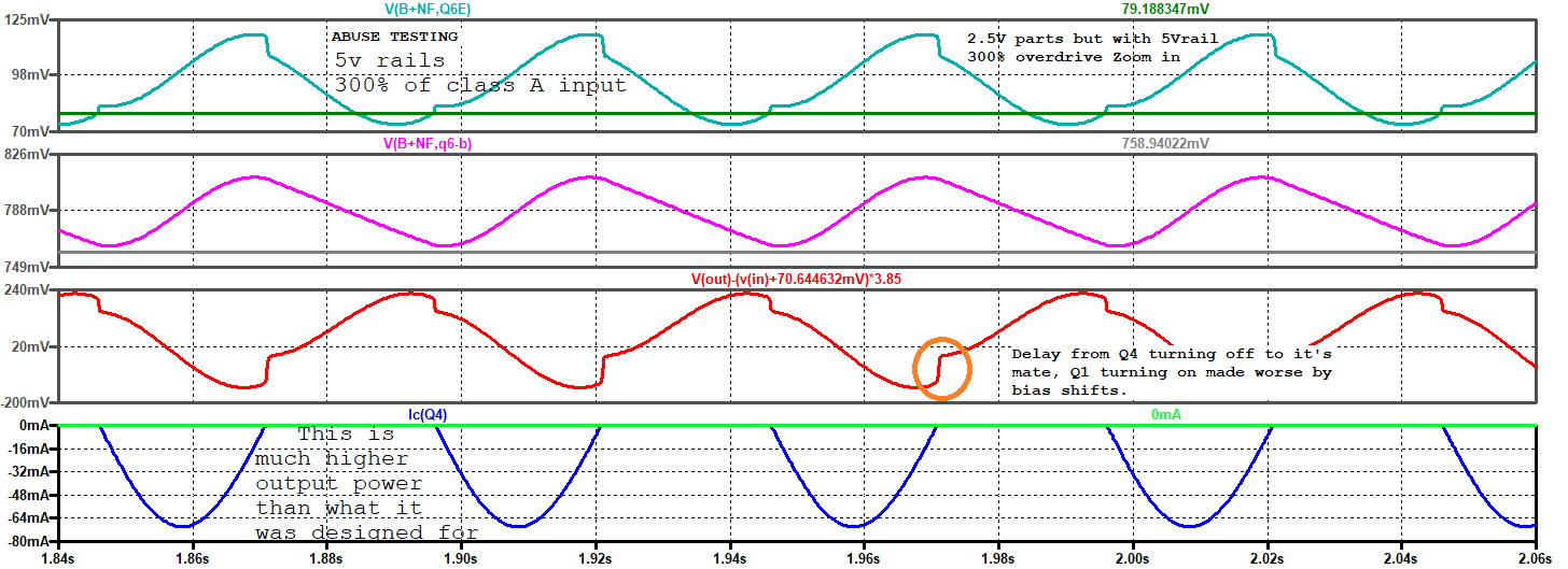
With an Abusive Drive level of 300%, the 2nd harmonic is still behaved, but all the upper harmonics are way too high in amplitude and the DC bias points are shifting too much. With these plots I was comfortable setting the class A DC bias point to 1/2 what was needed for 110dB at the ears to effectively double the battery life. If I set the bias point 2X higher, I'd have to charge the batteries twice a 60 hour work week instead of just on weekends. I don't listen to anything this loud nor do any of my friends so I'll take the longer battery life option.
N-Period=5
300% overdrive on the input 50mW into 30 ohms
or 117dB rms from 100dB/mW headphones.
Fourier components of V(out)
DC component:-7.2119e-008
Harmonic Frequency Fourier
Normalized
Number [Hz]
Component
Component
1
2.000e+01 1.731e+00
1.000e+00
2
4.000e+01 5.125e-03
2.961e-03
3
6.000e+01 4.023e-02
2.324e-02
4
8.000e+01 1.596e-03
9.222e-04
5
1.000e+02 2.325e-02
1.344e-02
6
1.200e+02 1.274e-03
7.363e-04
7
1.400e+02 1.613e-02
9.320e-03
8
1.600e+02 1.170e-03
6.758e-04
9
1.800e+02 1.216e-02
7.027e-03
10
2.000e+02 1.103e-03
6.374e-04
11
2.200e+02 9.607e-03
5.551e-03
Total Harmonic Distortion: 2.998221%(3.116022% )
In Stereo Review January 1989 pages 72-78, Ian G. Masters published testing on the audibility of distortion. With "Jazz, 4% THD distortion was audible and 1% really wasn't audible. On solo flue music, 1% THD distorion was audible.
In an older article on distortion, (I can't find it back, it was on Microfiche at the libary) what I remember was 1% 2nd distortion (1E-2 normalized) was considered mostly inaudible. 60dB (1E-3 normalized) 3rd was mostly inaudible and at much higher harmonics 80dB (1E-4 normalized) down harmonics was inaudible. The allowed even harmonic's sensitivity dropped 6dB/octave and the allowed odd harmonics dropped at 12 dB/octative. (We are more sensitive to symmetrical compression of the waveform (odd harmonics) than asymmetrical compression (even harmonics).) I really can't find this article back. If you have the name or a copy, please get it to me via an Audio Asylum Message.
On the SMT parts, use water or IPA soluble flux on every solder joint before the iron touches the board. This isn't the flux inside the core of the solder. This is additional flux you apply yourself through a small bottle.
After soldering, clean the PBA after soldering! 90% IPA works nicely, but clean it outside. 90% IPA is flammable, 70%, not as much. Clean even with no-clean fluxes. Some parts do not like being submerged in solvents: pots, switches, carbon comp resistors, aAluminum capacitors, non-hermetic Tantalum capacitors and some film capacitors. To be safe, super clean the board before putting on these parts on and then give it another spot cleaning before you conformal coat the PBA. (Printed Board Assembly)
Yes you can put one drop of Dawn dish soap in with your 70% IPA to help clean, but give it a rinse with pure 70% IPA after you are done scrubbing with the acid brush.
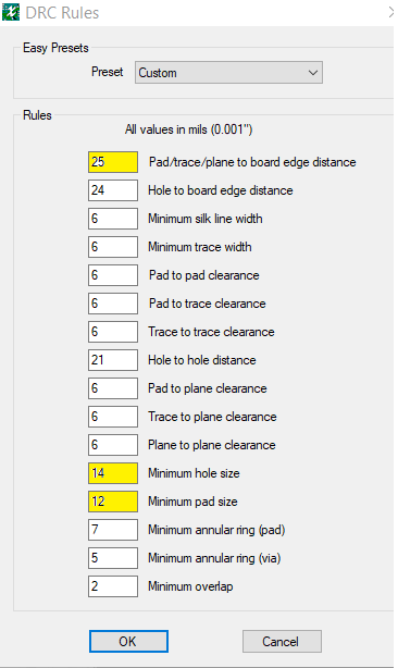
These are the settings I use in xCHECK when I check the ExpressPCB files. I avoid small holes and I allows small pads so I can use a small pad to put rounded corners on square cornered SMT pads.:

Zipped Care Package (17-Dec-2025) Not for Commercial
use. DIY use only.
Part Aging from the European Cooperation for Space Standardization (2010) A decent list of part value shifts.
https://www.edn.com/op-amp-dc-error-characteristics-and-the-effect-on-high-precision-applications/ Opamp fundamentals
First
version
14-Dec-2025, Last update 14-Dec-2025.
Changes to correct font or spelling issues won't count as an
update.
27_FEB_2026
added clarification that for +/- 5V, 8 batteries, the zener is
5.1V not 4.3V
.
 ( New 2024 index page.)
 _(
Old 2003 index page.)
_(
Old 2003 index page.)
 _( AMP Second index page.)
( Fancy index page.)
_( AMP Second index page.)
( Fancy index page.)
.