The interaction between rectifiers and transformers is well documented in math heavy technical texts, but it is not well know even amongst advanced hobbyists. With this site, I hope to fertilize your mind enough that you'll actually be able to read some of those technical texts and not fall asleep. So grab your coffee (forget the decaf) and stay awake as you read this.
Hint:
In Netscape or IE, I recommend that you type a CTRL-N to open a second browser window so you can look at the schematic at the same time as you look at the waveshapes.I want to explain:
1. That the output voltage is not usually sqrt( 2) time the rms secondary voltage.To add later:
2. The RMS current in the secondary winding can be much larger than the DC output current.
3. Snubbers do more than deal with the diode recover spike.
4. Even tube rectifiers can cause distortion and occasionally benefit from a HV snubber.
5. Point out how choke input supplies can also can have diode recovery problems even with tube rectifiers.
6. Why a large single cap and be almost as good as a pair of caps with a resistor in between them for the snubber.
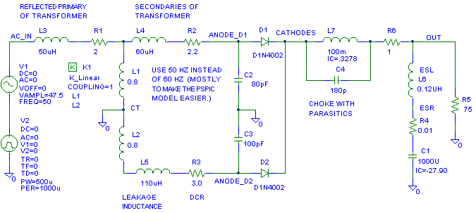
The transformer modeled below is an imaginary 60V RMS CT 1.0A 50 Hz transformer with 12% transformer regulation. This transformer is used in a full wave center tap capacitor-input supply.
R1 and L3 are the reflected primary side DCR and leakage inductance.I'm using a 60V transformer the example because the demo PSpice comes with a 100V 1N4002 diode model. The 1N4002 model in PSpice generates a smaller better behaved recovery spike than most real world 1N400x diodes I've used.
L2 and L2 are the inductance of the core as seen from each secondary.
R2, L4 and C2 are the parasitics of one half of the secondary.
R3, L5 and C3 are the parasitics of the other half of the secondary.C2 and C3 (80 pF and 100 pF) are the winding to winding capacitance, self capacitance and the winding to core capacitance all rolled in to one.The bridging capacitance from primary to secondary and primary to core have been omitted.
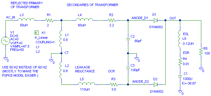
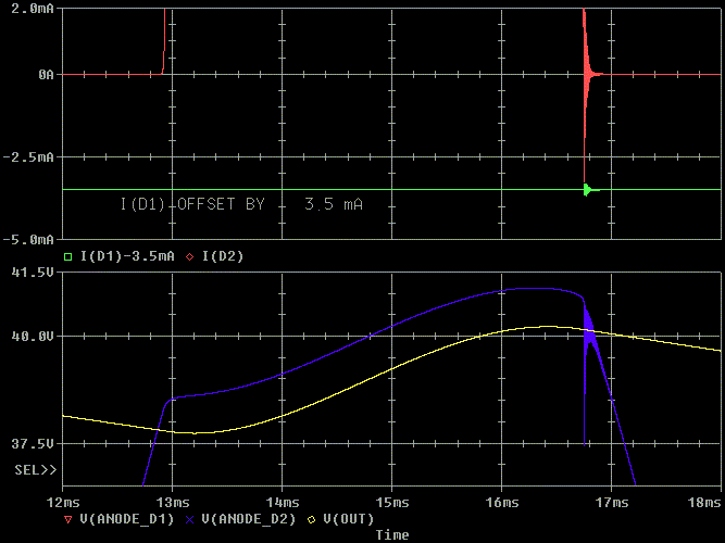
Look at the top plot. Ignore the ripple in the average and RMS, I don't yet know how to get rid of the ripple in the average and RMS show in the display.
Notice how the red I( D2) peaks much higher than the average output current blue I( R5). This is because the average load current is compressed to be delivered all at the crest of the waveform.Look at the bottom plot.All of the "charge" going into the capacitor for the half cycle of 60 Hz is delivered during this time. During the charging time, the current out of the diode also supports the load current as well as charging the capacitor up.Notice that the RMS current for the half secondary yellow RMS( I( R2)) is higher than the output current blue I( R5). This is because the peak charging current is higher than output current. RMS current is the square of of the average of the square of the current. This is why average reading meters are only good for pure sinewaves. You need a True RMS meter to measure this distorted current accurately.Notice that the average current for the half secondary violet AVG( I( R2)) is half that of the output current. This is because the half secondary only conducts half of the time.
Notice how both the top and bottom half of the blue V( Anode_D2) winding is distorted when compared to the V( AC_IN) input. This distortion is because the secondary windings share the impedance of the primary winding and what ever impedance there is back to the utility company. This distortion will be transferred to other windings in the transformer if these windings exist. This distortion can be an issue in windings like the filament winding used to power a tube.
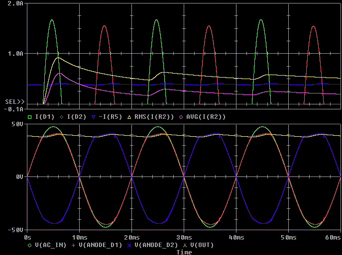
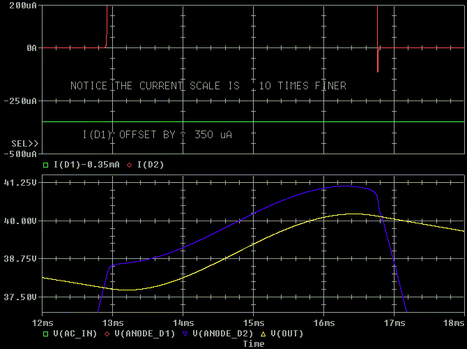
Next is a close up of the above image. Look at the first blue secondary voltage pulse and how it relates to I( D2).
Notice how the current red I( D2) starts to rise as soon as the secondary blue V( ANODE_D2) is a diode drop above the output voltage. This is where the diode is in forward conduction. Notice that the current also stops flowing once the secondary voltage is below the output voltage.Notice how much lower the output voltage yellow V( OUT) than the peak of the reflected green V( AC_IN) voltage.
In the ideal world, with a 47.5V peak secondary voltage, we'd expect the voltage on the capacitor to be a diode drop less than 47.5V or 46.8V DC. We have 39V DC. This is 8.5V lower or 7.8V more drop than a diode drop.
There is 2.6V peak to peak ripple on the output cap, 1.3V of this ripple would account would be a fair assessment voltage drop from the ripple. This leaves 6.5V unaccounted for.
So we have 39V out with a 0.4A load instead of 46.8V and 6.5V of it is missing.
Doesn't the extra 6.5V come from 0.4A flowing through 5 ohms (2 ohm
primary, 3 ohm secondary)?
But 0.4 A times 5 ohms is 2V. We are still missing
voltage!
6.5V/5 ohms is 1.3 amp peak. The load is 0.4A DC. Where is this 1.3A
peak? Look at the peak diode current. That is what causes the voltage drop
in the 5 ohm total effective resistance of the secondary.
.
The peak diode current is about 1.6A. The peak in the diode current does
not occur at the same time a the peak output voltage. This is the causes
difference between the 1.6A actual and 1.3A calculated peak current.
It is common to see the peak current in the diode 15 times the DC output current and the RMS current in the winding 3 times the DC output current. So if you buy a 0.4A RMS output transformer for your capacitive input 0.4 A DC output power supply, expect to have a red hot transformer! In this example, the peak current in the diodes is 7.5 (1.55A) times the average (0.2A).Now let's zoom in on the wave shape to look at those reverse recovery spikes. Once a silicon PN junction is forward conducting, it remains conducting for the reverse recovery time after it is reverse biased. It does not turn off right away. This causes current to flow back into the transformer from the output capacitor. When the diode does open up, it makes the LC tanks in the transformer ring.To precisely solve for the output voltage out of a capacitive input power supply and the winding currents is not as easy as it looks. O. H. Schade published curves to solve this problem back in 1943 in the Proceedings of the IRE, volume 31. You'll need to know the Secondary_Side_Equivalent_Resistance to use these curves.
The Secondary_Side_Equivalent_Resistance is the DCR of the secondary plus the primary resistance times (V_secondary/ V_primary) ^2
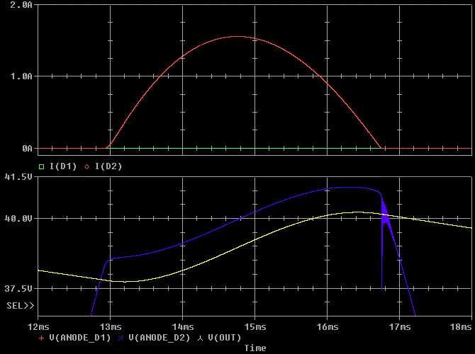
Now let's zoom in on the ringing in the diode current. I'll keep the voltage display the same for reference.
The initial spike in red I( D2) is from the diode's reverse recovery. The diode stays in the on state (a short) for a brief period of time after the voltage across the diode reverses. The slower the diode, the larger the current. The faster the diode, the lower the current spike. The rest of the ringing in I( D2) is from the parasitics of the circuit ringing.
The ripple in green I( D2) is from transformer coupled voltage ripple forcing current through the diode's internal capacitance. Keep in mind, I normally see 10 to 100 times more ripple than in this plot.
The ringing that occurs at about 16.7 msec contains harmonics that like to capacitively couple from the transformer to everything near the transformer and the leads going to the transformer.
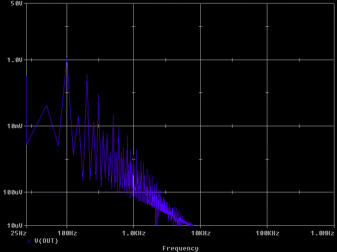
Lets look at the Fourier transform of the waveforms to see their spectral
content. The next plot is the spectrum of the output voltage. Keep in mind
that our ears can hear things too small for a typical oscilloscope to see.

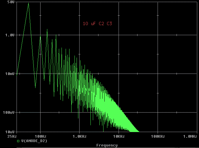
Now lets look at the anode of D2 using the same scale as the plot above:

With respect to a 1V signal, 1 mV is only 60 dB down. If this gets into the audio path. . .Ouch!
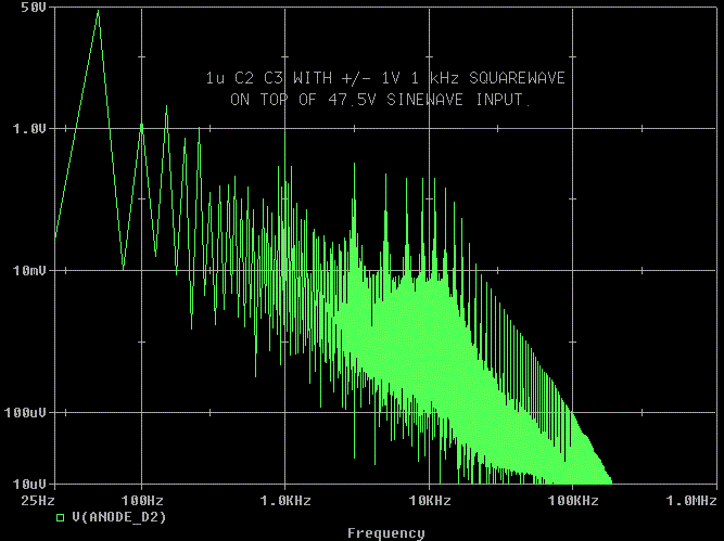
Now lets make C2 and C3 1 uF and keep everything else the same. Remember that second browser window I asked you to open? Use it to compare the before and after shots of the voltage. Notice the voltage ringing has disappeared.
Now lets make C2 and C3 1 uF

Lets look at a close up of the diode currents again. The reverse recovery
spike is much smaller. If I used the same current scale with out the 1 uF
capacitor, you won't be able to see it.
The spectrum analysis of the output voltage is not significantly
different.
The spectrum analysis of the anode voltage of D2 is greatly improved (quieter) except for a little increase at 10 kHz.
Note: If I add a few more parasitic losses like AC resistance, this peak at 10 kHz will drop.
Most of the reduction is at frequencies higher than the audio band, but
it becomes audible when it is run through a circuit with anything but
linear open loop gain. I don't know of a circuit with linear open
loop gain, not even a tube. It also becomes audible when it overloads a
gain stage because of that ringing.

Just to use up some bandwidth, I re-ran the analysis again with a 10 uF
capacitor for C2 and C3. This kills 10 kHz ringing.
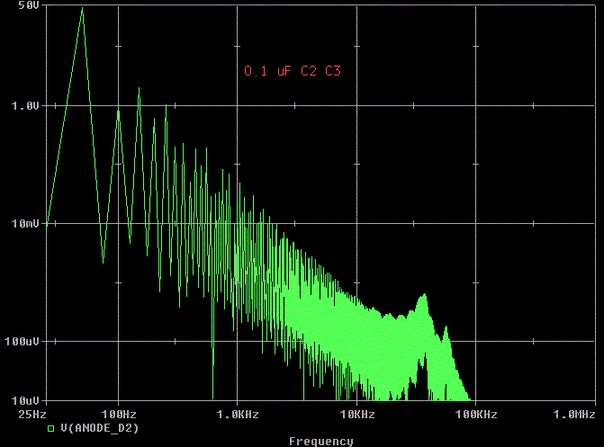
If 10 uF made it better, will 0.1 uF make it worse?
Yes. This is probably why snubbers don't work great in
all circuits. If the value is wrong, it can make it worse than it was
before.
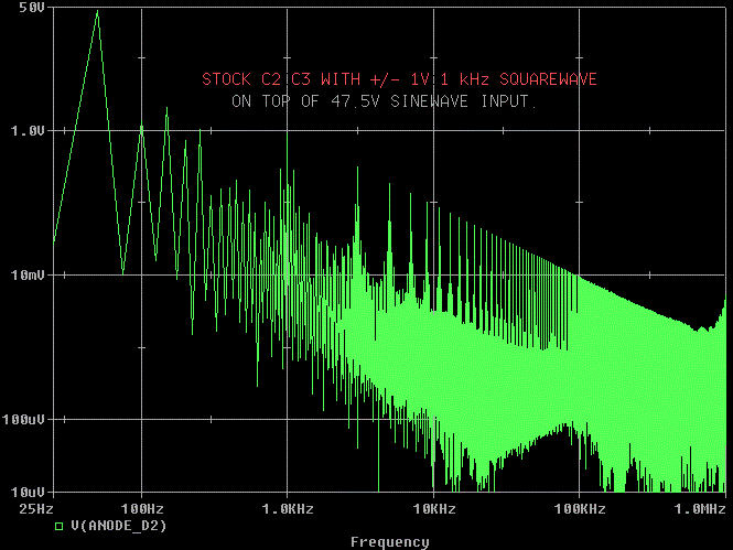
OK I had to mention snubbers didn't I. Lets add a 1V, 1 kHz square wave in series with the 47.5V sinewave to simulate some line noise. This is not a normal noise waveform, but many people understand a squarewave better than an impulse.
Filtering line noise is the other thing snubbers usually help with.
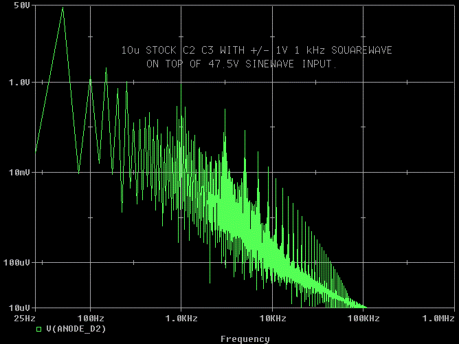
This is the stock V( OUT) with line noise added.
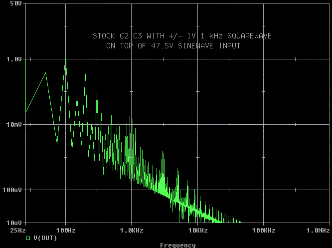
There does not look like there is a huge improvement on V( OUT)) when we
add a 1 uF on each diode.
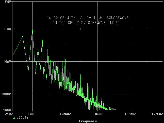
Remember, the transformer can conduct and radiate noise into adjacent
wire and parts. This is why even a tube rectifier can benefit from the use
of a snubber.
The 1u snubber looks much better than stock, but that pesky peak at 10
kHz is back.
So lets try 10 uF and see the peak goes away.
Yes, the peak went away. Usually larger amounts of farads in the snubber
will give larger amounts of attenuation. However, if we get too large,
we'll overheat the transformer.
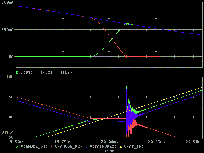
Let's use the same transformer at almost the same output current (less
output power) and look at the wave shapes.
Note: 100 mH is slightly larger than critical inductance.
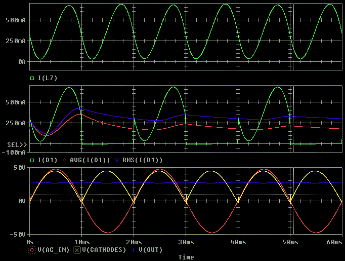
Notice that I( L7), the choke current has almost sinusoidal current
flowing it it at twice the 50 Hz line frequency.
The diode current I( D1) only carries the choke current for half the
sinewave. The average diode current is half the output current. But
because the peak diode current is lower, the RMS diode current is less
than with a capacitive input supply.
Notice the voltage spike at the zero crossings of the voltage of the
cathodes.
Let's zoom in on the crossover waveform and see that there is a lot of
ringing going on. Part of this is because I( D1) must charge up to the
current in I( L7) before the opposite diode I( D2) goes through reverse
recovery.
Let's add a 0.1, 1.0 and 10u snubber cap across C2 and C3. We again see
that the 10 uF adsorbs the most ripple because it has both the lowest
resonant frequency with the circuit parasitics and the lowest Q. If we add
additional RC damping to the circuit, we can get lower Q with smaller
capacitor values. This is covered on my damping ringing in transformers
web page.
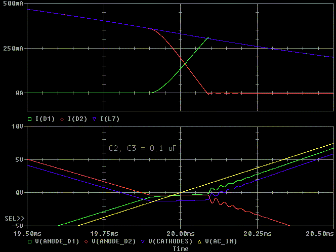
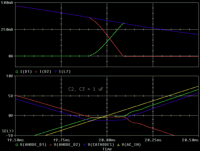

You usually have to double the value of the capacitance value to have a noticeable change in attenuation.
A physically large snubber cap can radiate lots of noise into near by wires and circuits.
Too big of a cap will overheat the transformer. 10 uF is 265 ohms at 60 Hz. 30V across 265 ohms is 0.11 A RMS. This is just at the "10% of rated current" rule for the largest uF size of snubber capacitor to use. The capacitor is to only draw 10% of the rated winding current. This 10% does not increase the RMS current 10% because it is out of phase with the output current.
For snubber voltages over 270V peak, add extra voltage margin in the part so that self heating and corona don't come into play and make the cap short out after a few hours to few months of use.
A snubber on a DHT is in the audio path. You'll need to use a fairly good capacitor for a DHT, but it does not have to be as good as the coupling caps you use in the circuit.
Two unequal caps in parallel in a snubber can have a resonance between them and make matters worse unless there is a resistor between the two capacitors. With closely spaced, equal value and size caps in parallel, the resonance usually self damps and does not occur.
I normally see much more high frequency ripple both on the anode of the diode and on the output voltage than what the model predicted.
I normally see much less ringing with a 0.1 uF capacitor than the model predicts.
Note: I'm doing these definitions from memory. I'll look them up later to make sure I agree with the books.
DCR
DC resistance. This term is usually used for the winding resistance of a transformer or inductor.AC resistance
This is the increase in winding resistance as the frequency goes up.ESLAs the frequency goes up, the current flowing in the wire starts to only flow on the surface of the wire. When the current only flows about 1 skin depth into the wire, we see the AC resistance climb higher than the DC resistance.
Skin Depth for copper is given by 7.5 cm/ sqrt( F in Hz).The skin effect and eddy current effect cause the resistance of a winding to increase with frequency. When wires are wound next to each other they generate eddy currents in each other. This makes the skin depth problem even worse and the frequency where the AC resistance starts to climb lower.
Equivalent series inductance. This term is usually used for the internal inductance of a capacitor.ESR
Equivalent series resistance This term is usually used for the internal resistance of a capacitor. This resistance is usually strongly frequency dependent. It will be highest near zero hertz and in the RF region.Secondary_Side_Equivalent_Resistance (I just made this term up.)There are two major losses in a capacitor, a series loss and a parallel loss.
At low frequencies, the parallel loss gets reflected to be in series with the actual ESR. This makes the measured ESR higher.At RF frequencies, the parallel loss is shorted out by the cap, but the actual ESR rises because of eddy current, skin effects and changes in the dielectric loss in the capacitor.
Secondary_Side_Equivalent_Resistance = DCR secondary + Reflected_DCR_PrimaryTransformer regulation (from memory)Secondary_Side_Equivalent_Resistance = DCR secondary + DCR_Primary * (V_RMS_secondary/ V_RMS_primary) ^2
Lets use a 60V 1.0A transformer with 12% regulation (120V primary) for an example.Charge% Regulation = 100% * (V_no_load - V_full_resistive_load)/ ( V_full_resistive_load)
12% = 100% * (67.2 V - 60 V)/ 60 V = 100% * 7.2 V/ 60VV_no_load = V_full_resistive_load * (% Regulation/ 100% ) + V_no_loadV_no_load = 60V * (12%/ 100%) + 60V = 67.2 V rms no loadThe peak of the unloaded voltage is sqrt( 2) * V_rms_no_load67.2 V rms * sqrt( 2) = 95 V peak end to endFirst notice that the unloaded voltage is higher than the loaded voltage. It is pretty much standard that the resistively loaded voltage is what is specified on a 60 Hz transformer. It is done this way so that under load (where we use the transformer), the loaded voltage is closer to being correct.
95 V/ 2 = 47.5 V half winding peak, no loadAs a rule at 60 Hz, the smaller the transformer, the worse the regulation. I have purchased transformers the size of my fist that had 30% regulation. This means our 60V transformer would read 78V unloaded. Regulation is important. The sad thing is that most transformers manufactures do not advertise regulation in their specifications. (For signal transformers, regulation is called insertion loss.)
Notice that the load current is not used in the regulation equation. When we know the load current, we can calculate the secondary sides equivalent resistance of the transformer.
Secondary_Side_Equivalent_Resistance = 7.2V/ 1.0 A = 7.2 ohms from the regulation specification.It is common for the reflected primary to have lower ohms than the secondary. This is because the primary must carry both the load current, the magnetization current and core loss of the transformer.
Part of this resistance is the secondary DC resistance, DCR
Part of this is the reflected primary DCR.Secondary_Side_Equivalent_Resistance = DCR secondary + Reflected_DCR_PrimaryThe DCR reflects from primary to secondary using this method:Reflected_DCR_Primary = PRI_DCR * (V_no_load_secondary/ V_pri )^2So we have 7.2 ohms - 2 = 5.2 ohms in the secondary. I'll use 2.2 ohms in one half. 3.0 ohms in the other.
2 ohms = 10.5 ohms * (52.5 V/ 120 V)^2At 50/ 60 Hz the leakage inductance of a fist size transformer usually does not get into the regulation equation. Leakage inductance does affect how much noise we get from diode recovery. If the leakage inductance is 150 uH, the 60 Hz impedance of the leakage inductance is:
XL = j * 2 * PI * 60 * 150 uH = j 56.5 milliohm56 milliohms is small compared to 5.2 ohms. So we'll ignore it for now for the low frequency calculations.Part of this leakage inductance will appear in the primary, part in each secondary. With a center tapped transformer, the two halves of the secondary will usually not have the same leakage inductance nor DCR.
Charge has the short hand symbol of "Q" and is measured in coulombs. 1 coulomb equals 1 amp of current flowing for 1 seconds.CoronaFor a DC signal:
Q = I * TFor an AC signalQ = integral of I(t) dt.For a capacitor:Q = C * VInto a capacitor where the voltage is not significantly changing:
Energy = 0.5 * C * V * V in joules.The charge into the capacitor equals the charge out of the capacitorThere are many tasks that are easier to explain by calculating charge than calculating current and volts.The average current into the capacitor equals the average current out of the capacitor.
Corona is what happens when the electric field gets high enough to rip electrons out of the air (or the what ever gas is around the electric field.) Almost all organic solids will have some entrapped gas. It only takes one defect in a 1000 square inches of insulation to cause a failure at high voltage.Corona can eat through insulation and cause a nasty failure. Corona attacks insulation through heat, corrosive gasses and by acids. Acids occur when the corrosive gasses from corona combine with humidity and make an acid. The part does not have to feel wet for acids to build up and cause a problem!
In clean un-ionized air, corona occurs at about 325V peak between smooth surfaces and about 270V peak between a needle point to a smooth surface. Above this voltage, there is a complex curve to determine where corona will start (Paschen's curve.) Some people use 75V/ mil (75V/ 0.001") as the actual break down voltage for air. Others use different formulae.
Once corona has started, it will continue to occur far below the inception (start) voltage. This is because there already are free electrons floating around waiting to cause some more trouble. Just add a little E field to the free electrons to accelerate them, they hit an atom, knock a few more electrons free and we have a problem.
One of many catch 22 problems with corona is that if you don't add the insulation or potting correctly, it can make things worse. However, you will always need insulation and potting if you don't want other types of failures in the transformer.
Also, just because you are far below 270V peak, don't think you can't start or maintain an arc or have insulation failures. Even fuses can have a hard time clearing because of arcs at voltages far below 270V. Even the 120V coming into the house can have voltage spikes and surges that can start corona or an arc. Also, there are other failure mechanisms than air breakdown (arcing) and corona.
The electric field that forms corona must be calculated using instantaneous voltage gradients. The electric field is NOT voltage divided by distance. Voltage/distance only works between infinite flat planes or very rounded surface.
One rule of thumb for benign environments is 20V/ mil (20V/0.001") across a clean surface and 50V/ mil through an undamaged insulator. Rules of thumb do not always work, but they are a good starting point.
So for 500V peak, we'd want 25 mils minimum spacing and 10 mils of insulation for a piece of metal with no sharp outward points. The trick here is the three concepts: clean, minimum spacing and no sharp points. If you clean a surface till it shines and then let it collect dust or finger prints, it isn't clean any more. Keeping it clean is one reason why you wear clean gloves when handing the raw materials.
 ( New
2024 index page.)
( New
2024 index page.)
 _( Old 2003 index page.)
 _( AMP Second index
page.)
_( AMP Second index
page.)
 ( Fancy index page.)