This trick for delaying B+ is NOT recommended for
beginners.
If the layout below does not make sense to you, you're
not ready to try this.
Both of my amps has this circuit installed in it.
They have been working fine for weeks (update: Months
and has survived an arcing tube).
This does not change the sound of the amplifier, it just helps the tubes last longer.
These notes and mods are for the
original amp sold in year 2000 ONLY!
I don't have a clue if
they will work in the current production amps.
I don't know how to
determine what version amp you have.
If you break it, you fix
it.
This involves working with high voltages,
attempt this at your own risk.
Added 01/30/01 Updated 02/16/01
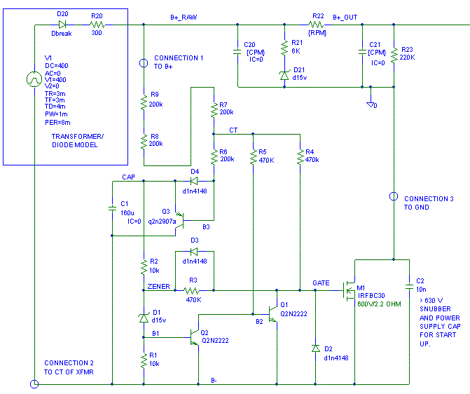
The FET I used in the PSPICE circuit below is a low on voltage, but it is the only FET that I have a PSPICE model for at the moment that is close to being the right part. I am using a simple model for the transformer so that it only takes about 11 minutes on an AMD K6-II 475 MHz machine to run one sweep of the transient analysis. (Yes I said minutes, not seconds.) If I don't use the simple model, it seams like it takes 3 times that long. (Transient analysis settings are at 1 msec print step, 3 millisecond maximum step size.) All resistors are metal film 1/4 W. No heatsink is needed on the FET, but the FET should be screwed to the protoboard it is used on to keep it from shorting to things it should not short to. Do not let the nut touch the body of the FET while tightening the screw, it can damage the FET.
NOTE: You need to use a 1000V FET for M1 and a 1000V cap for C2 if the switch is to be used above 450V peak.
How it works:
* C2 stores some energy between line cycles to power the circuit and C2
protects M1 from some spikes during its on/off transition. If C2 is too
big in uF, M1 will be damaged when M1 turns on. If C2 is too small, the
circuit will never turn on.
* At first application of 115V to the power transformer, C1 = 0V which
keeps D1 at zero current flow. D1 at zero current flow keeps Q2 off. Q2
being off lets R5 turn Q1 on which keeps M1 off.
* C1 slowly charges up. When C1 charges up far enough, D1 starts to
conduct and turns Q2 on. (R1 sets the bias current for D1's turn on
point.) When Q2 turns on, Q1 gets turned off and the gate on M1 rises. R3
and R2 provide hysteresis to help make Q2 snap on and stay on
until B+_RAW is charged. Both R3 and R4 pull the gate of M1 high to turn
M1 on.
* D1 is a 1N5245B
* D3 clamps the gate voltage to about 16V, (a bit high, but high voltage
FETs generally have >20V gates.)
* D2 protects Q1 from ringing negative far enough to damage Q1.
* D4 protects the base emitter junction of Q3 from reverse bias.
*** At power down, when D1 can no longer be forward biased, Q2 turns off
which turns Q1 on which shorts out the gate of M1 (turns M1 off.) R2 and
R3 provide hysteresis to help make M1 snap off cleanly.
*** After Q1 turns on, Q3 is biased on through a trickle current path
through R6 and R5/ R4 to discharge C1 quickly for the next power on delay.
Any voltage on B+_RAW will limit the amount C1 can be discharged.
*** If C2 is too small or C20 is too big, C1 may get turned on in normal
operation and the B+ will not start up gracefully. If R4 and R6 are too
small in value, Q3 can draw too much current from C1 and Q3 could be
damaged. Too small is less than 15K ohm total.
Lets look at the waveforms at power up.

We can see that with a fully discharged C1, we get about a 15.5 second turn on delay. The leakage current from C1 will make this delay longer. If C1 becomes too large in uF, it will be too leaky for the circuit to work. Even though there is less than 20V on C1, I would use at least a 35V part here to keep the leakage current low. Buy C1 on life expectancy. If a 50V part is 2000 hours and a 35V part is 1000 hours, buy the 2000 hour part. If you can fit a 5000 hour part on your board, use it over a 2000 hour part.
Because C2 gets discharged before B+_RAW is charged up, Q3 turns on for a little while to discharge C1. That is why there is a dip on the C1 capacitor voltage (CAP) when the gate goes high.
Now lets see the waveforms at turn off:
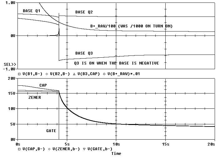
Because the capacitor does not get fully discharge (it only gets down to about 5V), we will loose about 4 seconds worth of delay if the power is turned off for 10 seconds and then turned back on. This is acceptable in my book.
This is the first cut at my layout. I added a 2K resistor in the gate of the FET to function as a grid stop resistor. This is presently not shown in the schematic above.
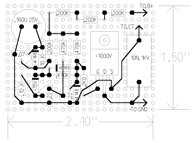
* I wanted a shorter delay than 16 seconds, so I used 100 uF (50V)
instead of 160 uF (35V). According to the model, the 160 uF gives almost
16 seconds delay and the 100 uF about 10 seconds delay.
* The 2.0K go the gate of the FET ended up being a 2.2K.
* I cut the protoboard slightly larger than the layout.
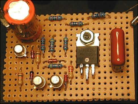
* I used some of the JAN metal can transistors I have been saving for a
special occasion instead of a PN2222A and a PN2907A.
* Some of the part markings were erased from me scrubbing the flux off
with acetone (no spark sources nearby!!!).
* I cleaned the board before I installed the capacitors so I would not
damage the capacitors.
* The board around the power FET's middle pin must be perfectly clean.
(The FET was an IRFBG20, 1000V, 11 ohms from Digikey.)
** Do not let the nut touch the FET when you tighten the screw. It will
put enough pressure on the FET to crack the body of the FET and damage the
FET.
With 45V applied between the schematic node called "CT" and "B-", the gate goes to 15V (turns on) after a verbal count of 22. With the 100 uF capacitor removed, the gate goes high at 34V on "CT" and goes low with 24V on "CT". The 100 uF capacitor is fairly rapidly discharged when the 45V on "CT" is open circuited. So far, the circuit is working like the Pspice model.
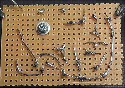
I installed the first board into one of my Paramours using stiff mounting wires as shown below:
I threw the power switch and nothing happened for 12 seconds and then everything came up! It worked. There were no nasty sounds from the speaker or tubes when it was used with the either original 2A3s or the AVVT 2A3s. With the turn-on delay installed and the AVVT 2a3 in the output tube socket, the scary buzz the speakers made at power up went away. With no turn-on delay, the stock 2A3s did not make a noise at power up but the AVVT 2A3 mesh plate did.
There was about 0.4 V DC 0.7 V AC across the FET during normal operation.
I noticed no change in the sound stage or noise levels from adding the delay. It actually seemed a little quieter. The 11 ohms in the FET could be adding some extra resistance for the snubber to work with.
It was very difficult to mount the delay so that the wiring from the delay did not short to anything else in the B+ supply. In the near future I will be using some non-acidic RTV to glue the board in place to prevent shorts. Now I've got to build the second board for the other channel! I'm tempted to glue an piece of protoboard over the solder joints to help prevent any potential shorts.
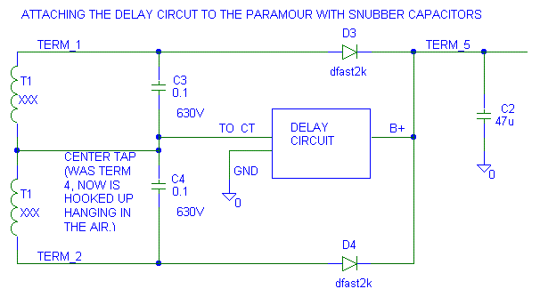
The delay circuit above could be used with an inductive input supply if a diode is added as shown in this link. I have not modeled this version yet to check the value of C2, but the concept is reasonably sound.
I am working on a higher voltage version of this that could be used with
a 700 V RMS winding feeding full wave bridge. I need this circuit for a
choke input circuit I am working on. Things are going very slow right now.
My goal is to post it Summer 2002.
All the parts for this circuit were purchased from Digikey except for the ones that came from my junk box. The parts that I found in my junk box are available at Digikey too.
 (
New 2024 index page.)
(
New 2024 index page.)
 _( Old 2003 index page.)
 _( AMP Second index page.)
 ( Fancy index page.)