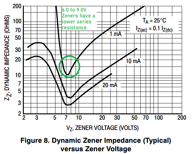
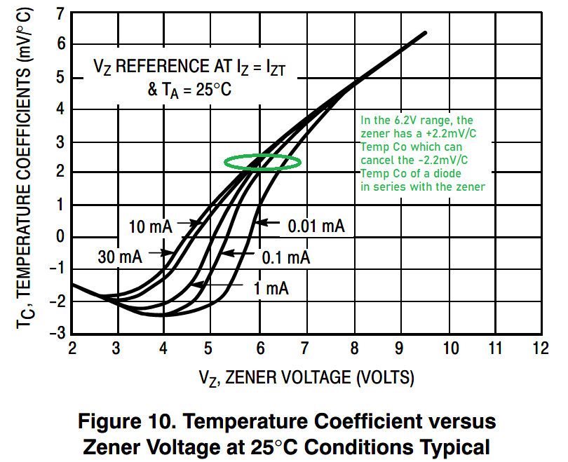
In the table below, I marked what I felt were good values in bold and acceptable value in italics. These data points were taken from the Q3/1988 Motorola "Rectifiers and Zener Diodes Data" book.
In the two Families of zeners shown below, one is a 1/4W family and the other is a 1/2W family.
| Nominal Zener voltage | Family_1 1/4 watt | Family_2 1/2 watt | Family_1 Vr test | Family_2 Vr test | Family_1 uV/sqrt(Hz) at 250 uA (Table) | Family_2 uV/sqrt(Hz) at 250 uA (Curve) | Family_1 Zzt @ 250 uA (Table) | Family_2 Zzt @ 250 uA (Table) | Family_2 Zzt @ 1 mA (Curve) | Issues |
| 5.1 | 1N4625 | 1N5231B | 3.0 | 2.0 | 2 | 1.5 | 1500 | 1600 | 200 | Poor Regulation |
| 5.6 | 1N4626 | 1N5132B | 4.0 | 3.0 | 4 | 4 | 1400 | 1600 | 100 | Poor Regulation |
| 6.0 | N/A | 1N5133B | N/A | 3.5 | N/A | 50? | N/A | 1600 | 15 | Unknown Regulation / Availability |
| 6.2 | 1N4627 | 1N5234B | 5.0 | 4.0 | 5 | 150? | 1200 | 1000 | 9 | Best compromise |
| 6.8 | 1N4099 | 1N5235B | 5.2 | 5.0 | 40 | 200? | 200 | 750 | 9 | Fam_1 Noisier
by 18 dB! |
| 7.5 | 1N4100 | 1N5236B | 5.7 | 6.0 | 40 | 400? | 200 | 500 | 12 | Noisy |
| 8.2 | 1N4101 | 1N5237B | 6.3 | 6.5 | 40 | 700 | 200 | 500 | 15 | Noisy |
| 8.7 | 1N4102 | 1N5238B | 6.7 | 6.5 | 40 | 900 | 200 | 600 | 17 | Noisy |
| 9.1 | 1N4103 | 1N5239B | 7.0 | 7.0 | 40 | 1000 | 200 | 600 | 20 | Noisy |
| 10.0 | 1N4104 | 1N5240B | 7.6 | 8.0 | 40 | 1200 | 200 | 600 | 25 | Noisy |
| 11.0 | 1N4105 | 1N5241B | 8.5 | 8.4 | 40 | 1600 | 200 | 600 | 30 | Noisy |
| 12.0 | 1N4106 | 1N5242B | 9.2 | 9.1 | 40 | 2000 | 200 | 600 | 35 | Noisy |
In the Family_2 noise curves, it was very difficult to read the values from the curve between 6.0 and 7.0V. This is because the curve is changing so fast. Every time I held the calipers against the curve, I got a different value. So I just used the tabulated curves from Family_1. From the Family_1 curves we see that the noise gets bad fast at 6.8V and above. This says we should use a 6.2V zener or lower for noise reasons.
Using a 6.2V zener in a current source we see by at Q1, R1 will have 5.6V across it. 5uV of noise out 5.6V is 121 dB down (very respectable). 150 uV out 5.6V is 91 dB down, still not too shabby.
If we used 4V drop for the gate of a FET, 150uV out of 2.2V on R2 is 83 dB down. 83 dB down isn't terrible, but it isn't great either. However, we don't use a single 6.2V zener and the gate of a FET for a CCS, we use two in series. We don't use one 6.2V zener because of regulation and output impedance and the gate threshold variation of the FET.
The zener voltage can change +/- 0.31V for a 5% part. The gate voltage can change more than +0.5 volt between power up and stabilizing in voltage and up to +/- 1V from FET to FET (at room temperature.) I'll use +/- 0.5V to be more reasonable for I've never seen +/- 1V on a FET that wasn't damaged. This means the voltage that sets the current can vary from 1.39V to 3.01V a 1:2.16 initial variation and up to 35% temperature variation. This much variation is not acceptable.With a transistor and one 6.2V zener, the current variation is more like 1:1.12 and the temperature variation will be closer to 4.5% (for a 60C change). With two 6.2V zeners and a FET, the variation is 1:1.30.


---
 ( New
2024 index page.)
 _( Old 2003 index page.)
 _( AMP Second index
page.)
 ( Fancy index page.)